This thread has been locked.

If you have a related question, please click the "Ask a related question" button in the top right corner. The newly created question will be automatically linked to this question.

TPS73001 reverse current limit

Genius 3900 points

Hi there,

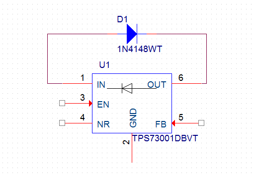
We use TPS73001 to generate 2.5V from 5V input, 50mA. 

As reverse current is not internally limited(Section 8.1.5 of datasheet), how could we implement external circuit to prevent/limit the reverse current, during power down? 

Could you please suggest some practical demo circuit on this?

Thanks.

  • Hi ,

    There are several methods to limit reverse current.

    The most common is placing a diode in parallel with the LDO. This will provide a robust path for reverse current outside of the LDO; however, PSRR may be degraded slightly due to leakages through the diode.

    You could place a diode before the input capacitor or after the output capacitor. The trade off of before the input capacitor is that you would still have reverse current until the input capacitor charges up, but you would protect the upstream components from the reverse current. The trade off for after the capacitor is that you will have to account for the diode drop when setting the output voltage (for an adjustable LDO, the FB network should be before the diode).

    Another option could be to implement an external active pulldown circuit to discharge the output when the LDO is disabled. To do this you would use drive the gate of a FET with the same signal as EN and when EN goes to logic low, the FET would discharge the output. This would prevent reverse current but will likely be the largest solution.

    Very Respectfully,
    Ryan
  • Hi Ryan,

    for the first paragraph, "The most common is placing a diode in parallel with the LDO". 

    (1)If we connect diode like following picture, there will be a direct-through current path in D1 under normal operation when Vin-Vout>0.7V.  LDO will be by-passed.

    (2)If D1 is reversed (with its anode connect with OUT) , D1 seems unable to block the reverse current from OUT to IN, because there could always be a reverse current path from the built-in back diode when Vin is lower than Vout during power down process.

    I do not understand. Could you please explain more ? Thanks!

  • Hi ,

    The correct configuration is your second statement. You are correct that the parallel diode solution will not block reverse current. A Schottky diode placed here will provide a robust path for the reverse current and protect the LDO from damage. This current will charge the input capacitor. Once the input capacitor is charged, you will no longer have reverse current.

    Very Respectfully,
    Ryan
  • Thanks, Ryan. You mentioned Schottky diode, and I think I understand. Is there any information about the built-in diode of this IC? Such as its IF(max) and VF?
  • Hi ,

    The body diode within the pass element of the LDO is an intrinsic diode and has not been characterized.

    Very Respectfully,
    Ryan