This thread has been locked.

If you have a related question, please click the "Ask a related question" button in the top right corner. The newly created question will be automatically linked to this question.

TPS53355 Layout of Ripple Injection circuit

Guru 20090 points
Other Parts Discussed in Thread: TPS53355

Hello,

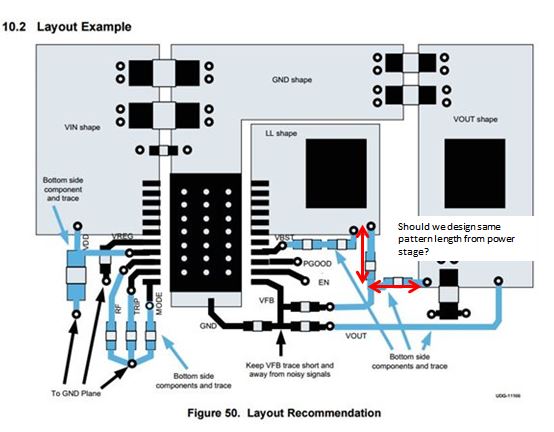
In the datasheet P.27, there is the description of "The AC coupling capacitor (C2 in Figure 38) should be placed near the device, and R7 and C1 can be placed near the power stage."

Are there any requirement without above?
For example, should we design R7 and C1 as same pattern length from power stage?


Best Regards,
Ryuji Asaka

  • I do not think the trace lengths are super critical. However I am a big proponent of symmetrical, well thought out layout. On the EVM the resistor and capacitor are placed very close together (adjacent). One end of the capacitor is connected directly to the VOUT copper fill. The resistor is connected to the SW node with a very short trace and a via up to the SW node copper fill. I think it is best to keep the trace lengths as short as possible for R7 and C1. the trace to C2 can be as long as necessary.
  • Hi John,

    Thank you for the reply.
    Could you please let me know the concern when the R and C layout is not symmetrical?

    Best Regards,
    Ryuji Asaka
  • I have not personally designed with TPS53355, so I do not know of any specific issues.  My comments were based on reviewing the known good EVM layout and my experience with designing many other dc/dc converters.  Typically we follow best practices for PCB layout and don't experiment much with poor or risky layout scenarios.  For this particular case, you are injecting ripple into the FB node.  You want to make sure there is a s little noise as possible, so minimizing the exposed etch near the SW node is a good practice.