This thread has been locked.

If you have a related question, please click the "Ask a related question" button in the top right corner. The newly created question will be automatically linked to this question.

TPS22910A load switch transition

Other Parts Discussed in Thread: TPS61291, TPS22910A

Hi ,

I have a Power multiplexing requirement with 2 Power sources and 1 output

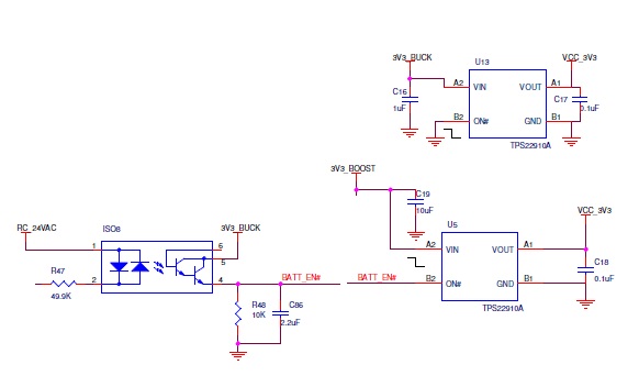
Primary source is AC-DC rectified 3.3V using Buck.

secondary source is Alkaline battery which connected to TPS61291 boost converter whose voltage will vary from 1.8 to 3.3V

Load requirement is 3.3V@210mA Max and decaps value is around 30uF at load.

When AC source is present,the system load should be supplied by AC and should switch to battery in case of AC absence.

We have used 2 load switches TPS22910A.

 Enable pin of load switch connected to AC source is by connected to GND and by default enabled.

Enable pin of Load switch connected to boost source is connected to AC detection logic using AC opto coupler to enable Load switch 2 before 3.3V completely shuts due to input capacitor and output cap hold time.

Could you please verify and suggest any modifications to attached circuit to enable smooth transition for 1.8V-3.3V input range of load switch2 ?

Will there be any problem during transition when Load switch input voltage is 3.3V and Load switch2 input voltage is 1.8V?

  • Hi Shankar,

    Thank you for all of the information you provided.  I understand the application and have one concern about the schematic.  When the AC/DC input is disconnected, is the 3V3_BUCK node floating?  If that is the case, then U13 may not block reverse current if the enable pin is always pulled down (keeping the part ON).

    While the TPS22910A blocks reverse current when ON, there needs to be a voltage differential between VOUT and VIN.  If VIN is disconnected and left floating, then it will follow the value of VOUT and there will never be a voltage differential measured.  VOUT and VIN need to be forced to different voltages at least 66mV apart for reverse current blocking to be active.  Please let me know if you have any questions on this.

    Thanks,

    Alek Kaknevicius

  • Hi Alek,

    Thanks for your reply.

    There will be 2 scenarios:

    1) Load switch 2 input voltage is 3.3V when Boost converter TPS61291 is in boost mode:

    When AC supply is removed,input bulk capacitor (100uF) after rectification will provide hold time to maintain 3.3V Buck for some time.

    Before Buck converter shuts and buck output cap discharges completely ,Load switch 2 will be enabled and will share the load along Load switch1, when VIN2 voltage is 3.3V.

    Once buck output cap voltage i.e VIN1 is less than system rail 3.3V by 66mV,then reverse protection will be enabled and only Load switch 2 will supply system load.

    2) Load switch 2 input voltage follows battery i.e 1.8V-3V  when Boost converter TPS61291 is in bypass mode:

    When AC supply is removed,input bulk capacitor (100uF) after rectification will provide hold time to maintain 3.3V Buck for some time.

    Before Buck converter shuts and buck output cap discharges completely ,Load switch 2 will be enabled ,but reverse protection will be enabled since VIN2 voltage is less than VOUT. This reverse protection will be on until VOUT decreases to voltage less than VIN2. Once VOUT is less than VIN2,Load switch 2 will supply system load.

    Once buck output cap voltage i.e VIN1 is less than system rail by 66mV,then reverse protection of Load switch 1 will be enabled.

    Is my understanding correct ? Do I need to make any modification?

  • Hi Shankar,

    I think the problem here would be leaving load switch 1 always enabled and leaving the input floating.  Until reverse current blocking is enabled, the switch is "closed", so VOUT will follow VIN and VIN will follow VOUT.  If VIN is disconnected and the output drops, then VIN will follow VOUT since there is nothing forcing the two to opposite values.  If VOUT is brought up (load switch 2 is enabled) then VIN will follow and no voltage differential will be measured across the load switch.

    Because the input of load switch 1 is disconnected, a voltage differential will not be measured between VOUT and VIN.  Therefore, the only other way to implement reverse current blocking is by pulling the ON pin of load switch 1 high (off) when input 1 is disconnected.  Is this possible?

    Thanks,

    Alek Kaknevicius

  • Hi Alek,

    To turn off load switch 1 when VIN1 is disconnected,I need to add schmitt inverter powered from battery to turn on-off load switch,but this would drain battery.

    The other option is to use Low forward voltage schottky diode instead of load switch1 and use only load switch 2 for battery path.