


I need some advice about the layout of the TPS54x25 switcher.
Assuming it's a 4-layers board, and the layer arrangement is: Top -- GND -- Power -- Bottom.
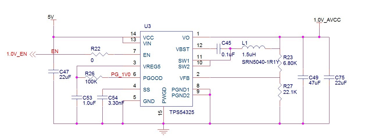
schematic:
layout:

1. about the layout of the output voltage signal connecting to the high side of voltage feedback resister, that is R23 in schematic.
I use a wide wire connecting R23 to the power polygon of the switcher output.
My question is :
Is it better that i directly place a via near R23 through to the bottom plane if the the power plane below the switcher and R23 is an integrated 1.0V_AVCC plane ?
2. about the layout of the ground signal connecting to the lower side of voltage feedback resister, that is R27 in schematic.
As the guidelines recommended, I use a wire connecting R27 to the signal ground pin of the switcher, and then connecting to the PGND.
My question is:
Is it NOT preferable that i directly place a via near R27 through to the PGND plane? The second layer is PGND plane.
This may be a little fussy, but i'm curious to know.

