Because of the holidays, TI E2E™ design support forum responses will be delayed from Dec. 25 through Jan. 2. Thank you for your patience.

This thread has been locked.

If you have a related question, please click the "Ask a related question" button in the top right corner. The newly created question will be automatically linked to this question.

LM5069

Other Parts Discussed in Thread: LM5069, LM5576, CSD19534Q5A

Hi team,

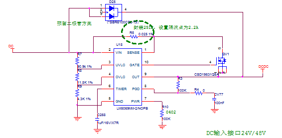
My customer wants to use LM5069 in their system, which is 24V or 48V input compatible. The schematic as below:

the output cap is 680uF, which is the input of a DC/DC (LM5576, 24V/48V to 12V/1A)

the MOSFET is CSD19534Q5A, instead of 19531

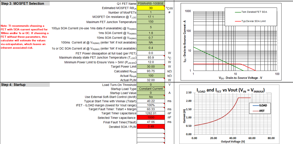
I used the calculate tool and found some result has high risk. I attached the excel sheet for your reference.

4786.Copy of LM5069_Design_Calculator_REV_B.xlsx

regarding the result, I have some questions:

1. what does the green trace/red trace in SOA figure stand for?

2. could you please explain the start up figure? If the output voltage already reaches 48V, why does the current clamped to 2.2A? the max load current was set as 1.3A.

3. How does the tool calculate the typical start time and target fault timer?

4. For customer's application, how to determine the power limit and timer cap? could you please suggust a proper value?

thanks:)

BR,

Mike

  • Hi Mike,

    These questions were addressed via our email conversation but to capture the high level answers:

    1) The green trace is the SOA curve from the MOSFET (values entered in step 3) which are then de-rated for higher operating temperature. The red trace is where the FET will be operating based on where the fault timer is set (step 4) and the power limit dissipation (step 3).

    2) Nearly all calculations in the tool assume worst case scenario which would be at Vin max (VIN = 60V, entered in step 1).

    3) The typical start time is calculated based on the equation in the datasheet. It is a function of the current limit, power limit, output capacitance. Target fault timer is the typical startup time + margin (to account for variation of the timer threshold and currents, the power limit tolerance, etc.).

    4) Generally, power limit is set close to a minimum to keep the MOSFET under minimal stress. Timer cap is set to be higher than the typical startup time + margin. However, some designs may not work with this and that is due to insufficient SOA of the MOSFET. Options would be to pick a stronger MOSFET, or use techniques to reduce stress such as a dv/dt circuit.

    We have an application note which discusses details of hot swap design at www.ti.com/hotswap --> "Technical Documents" --> "Robust Hot Swap Design" and video tutorials at www.ti.com/hotswap --> "Support & Training"

    Thanks!
    Alex