This thread has been locked.

If you have a related question, please click the "Ask a related question" button in the top right corner. The newly created question will be automatically linked to this question.

TPS63060 stability problems

Other Parts Discussed in Thread: TPS63060

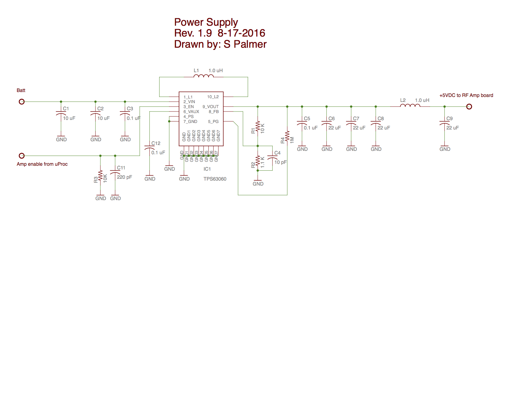
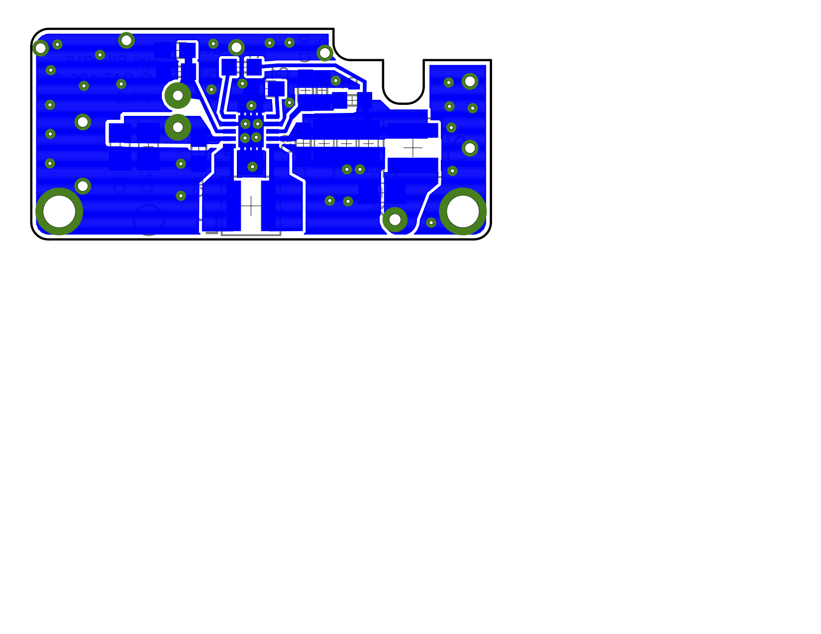
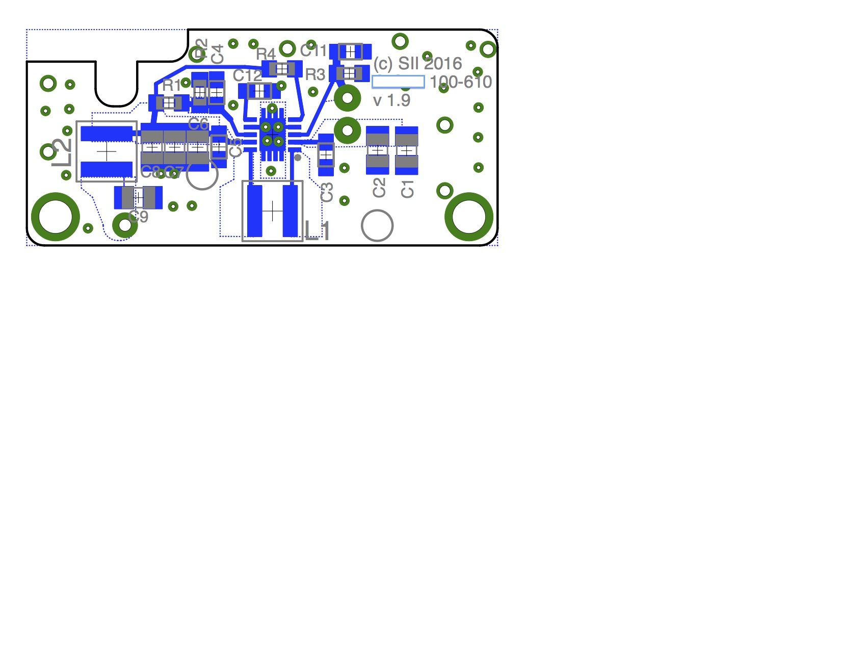
We are using the TPS63060 on a small circuit board to power approximately a 500mA load at 5.0VDC.  Supply voltage to the circuit can vary between 4.25 Volts to 6.8 Volts in application, however, in the below described test, the input voltage is always 6.0V.  We have carefully followed the design criteria in the documentation and have examined parts layout, component values and workmanship.

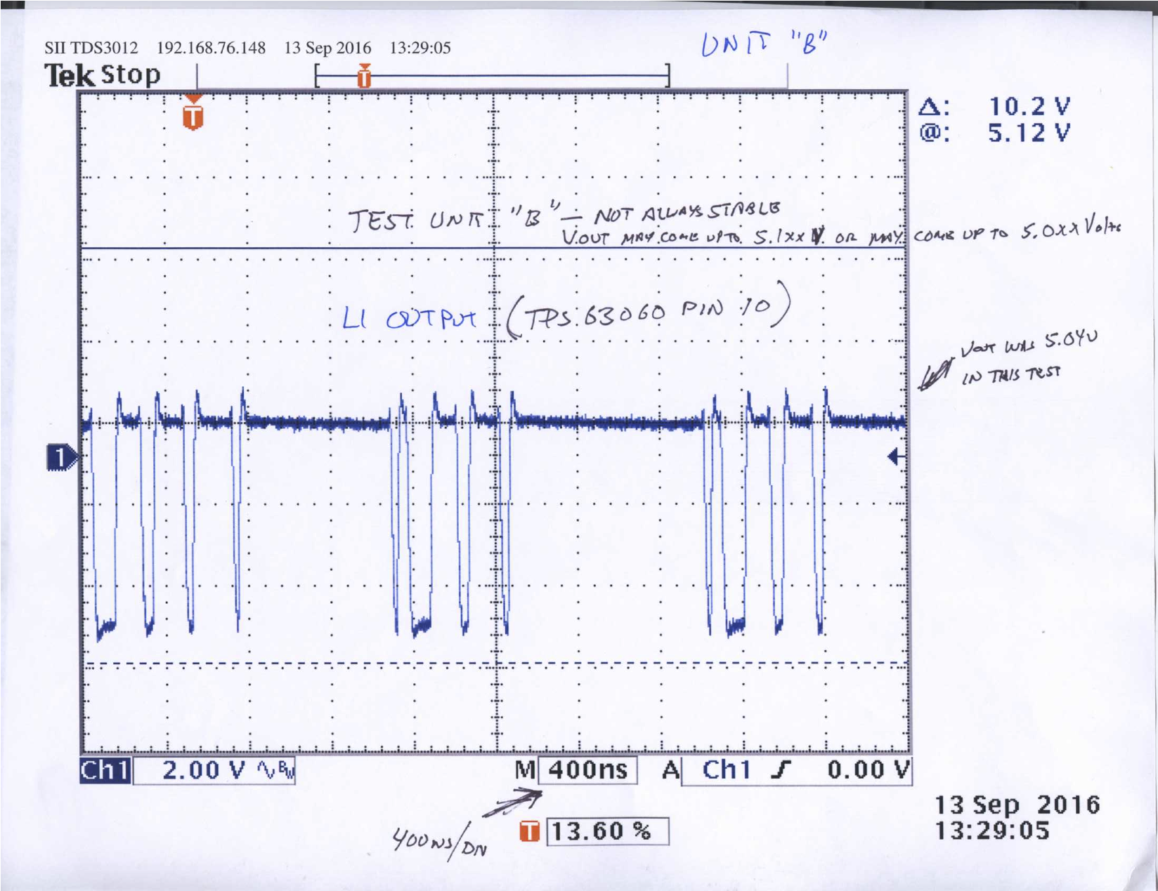
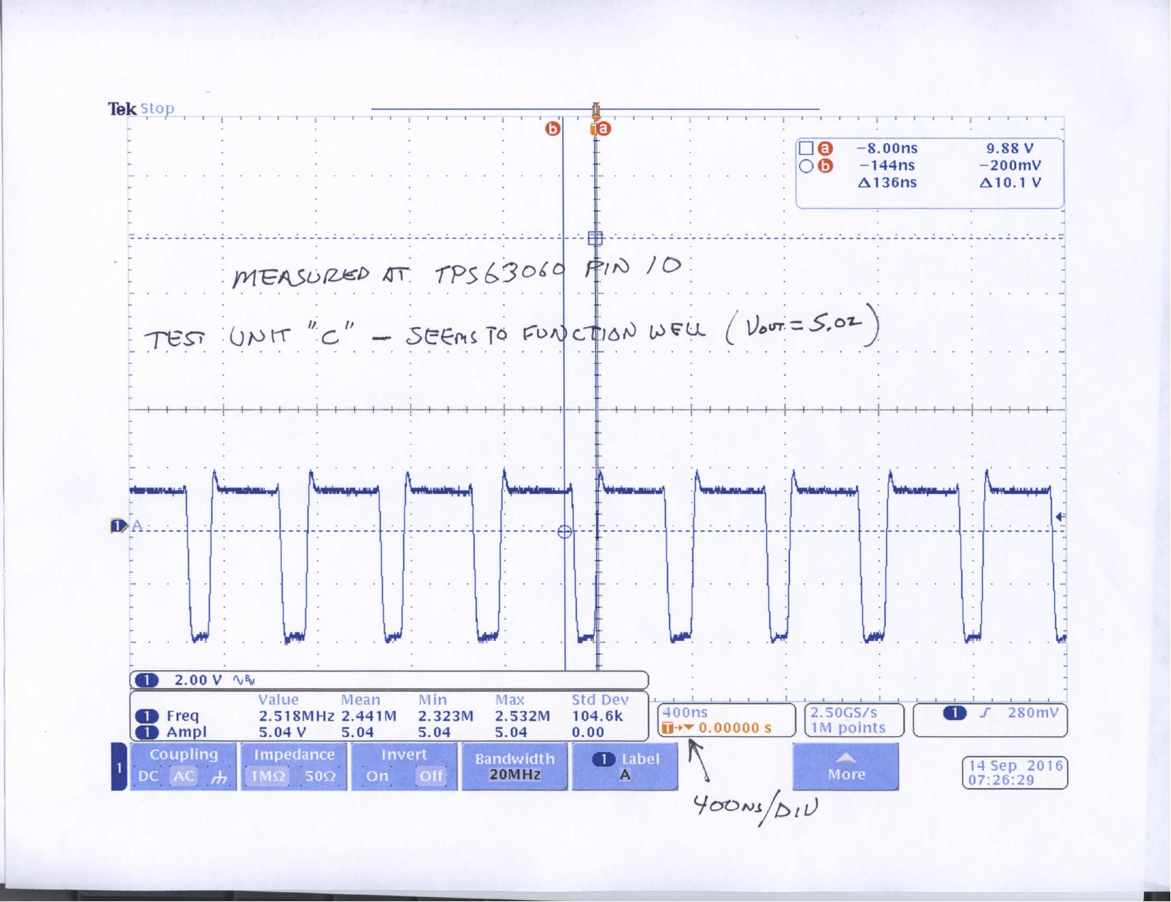
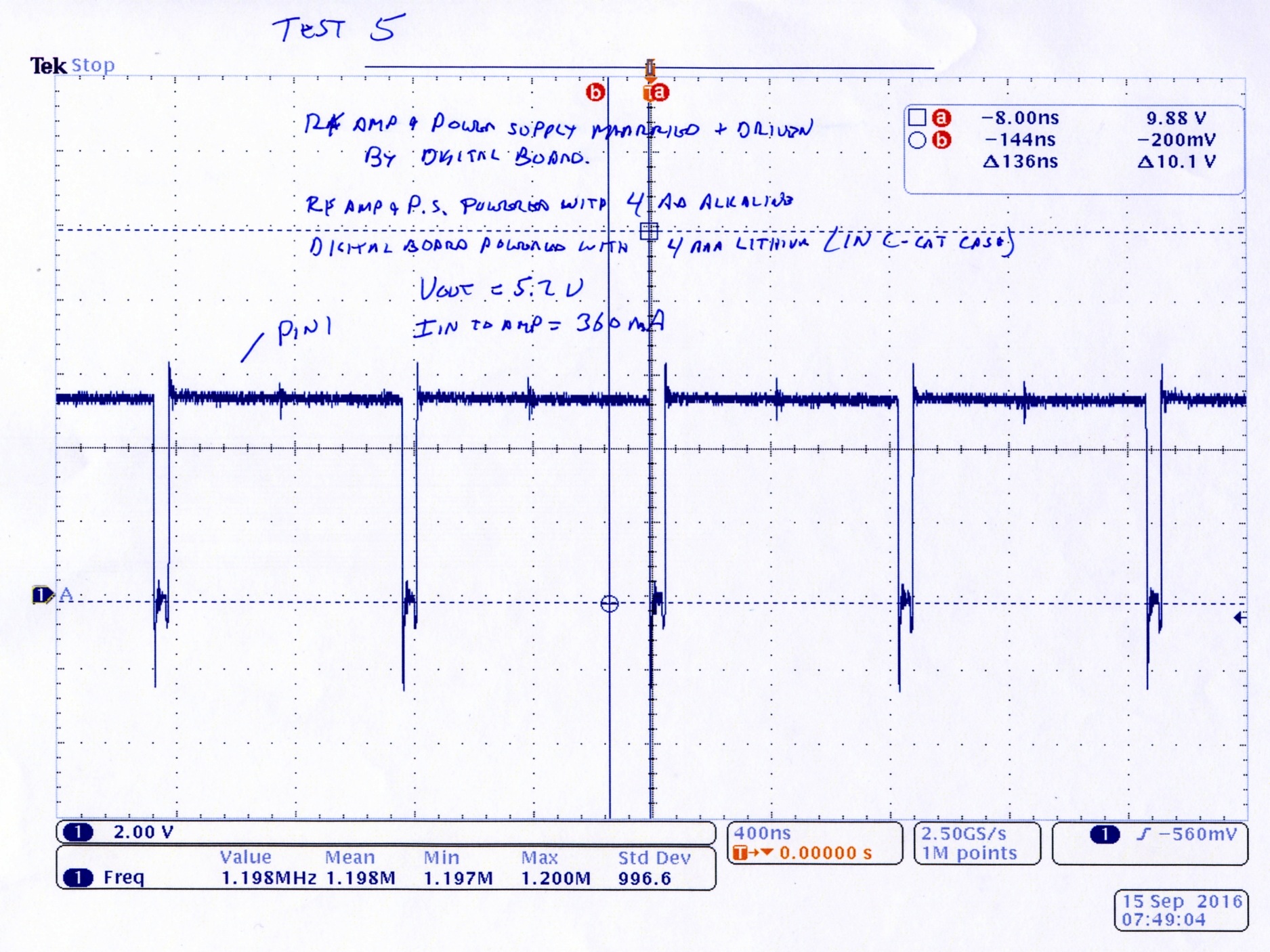
The problem:  Sometimes the buck-boost regulator will come up in an unstable mode with an output of about 5.1-5.2 volts instead of the desired voltage of 5.0V.  The TPS63060 also gets excessively warm in this unstable mode.  We have tested both low impedance voltage divider FB circuits (R1 =10K, R2=1.1K with 10pF across R2  (C4) and also with a value of C4 of 50pF) and high impedance voltage divider FB circuits (R1 =1M R2=111K with 10pF across R2.  If the device comes up in the unstable mode, we can sometimes "fix" it by touching a scope probe to the junction of R1 and R2 (FB input).  

Some of the circuit boards seem to work fine and others exhibit this unstable behavior.  We suspect that something in the design may be marginal and that the device is just on the edge of stability/instability.

We can send scope traces of waveforms on each side of L1 if this will be useful.

Please help!  We are temporarily stumped and must solve this!  Thanks!

  • 1. Can you share the schematic and the layout?

    2. To sum up the test conditions: Vin=6, Vout=5V and Iout= 500mA? Are you using a resistive load for doing this experiment?

    3. What is your application?

  • Sabrina,

    1. Here is the schematic and the layout.  The back side of our board is mostly solid copper.

    2. In application, and in testing and troubleshooting, this board is powered from batteries.  Nominal Vin = 6 V, but under load may drop to 5 or less.  Vout is 5.0V and Iout is about 500mA.  On the bench we're using 10 ohms of resistive load.

    3. In application, this power supply powers an small RF amp.  

    Because this board will be physically close to a 1W RF amp running about 160 Mhz, we chose lower values of R1 and R2 than the reference example in the data sheet to reduce the possibility of RF entering the FB input.  Initially we did not change the value of C4.  This was an oversight on our part.  We thought this might be a source of the stability problem, so we tried adding capacitance to bring C4 to about 50 pF, but didn't see an improvement.  We then replaced R1 and R2 with 1M and 110K and C4 with 10pf.  This did not seem to make a difference either.  We also tried tying PS to Vin (disable power saving mode) and to ground (enable power saving), but didn't see any change.  We assume this is because our load is about 500 mA and the TPS63060 is always running in PWM mode.

    I have included scope screen shots for two units measured at pin 10 on the TPS63060.  The trace for Unit C suggests to us that the unit is running at about 2.4 MHz, while the trace for Unit B perhaps suggests it may be running at about 700 KHz although we are not that familiar with "correct" or normal operation.

  • Thank you for sharing the details, can you post the silk screen too?
  • Hi Sabrina,

    Thanks for your reply.  We really appreciate and need TI's help.

    We have tried a number of things since yesterday and so far none have solved the problem.  Here is the board with silkscreen shown (but without copper floods shown).

    The power supply board, as shown below and in previous posts, is married back-to-back with the 1W RF amp board.  The RF amp draws about 360 mA at 5 V.

    The boards we're testing are first production boards.  Of about 10 we've tested in fully assembled devices most seem to work fine, but we're concerned we might be on the ragged edge of stability (or have some other problem).  We first noticed this problem when a few transmitters output 1 W of RF at power on and then drooped to about 900mW of RF power over 30 seconds.  When we investigated, we found that Vout from the power supply was starting at about 5.2V and then dropping to 5.1 or less.  The FB resistors we're using should set Vout to 5.0 volts.  The transmitters that seem to work well start with Vout on the power supply at 5.0 v plus or minus 50 mV and show no change in Vout over time.  

    If we replace our load (the 1W RF amplifier) with a 10 Ohm resistive load, the power supply seems to operate correctly. If we add 10 ohm resistive load in parallel to the RF amp load, the power supply seems to behave correctly.  We tried adding various values of resistive load while the RF amp was connected as a load and found that 68 ohms seems to correct the problem as well, but higher values did not.

    We have PS enabled and in referencing the data sheet (Figure 10, on Page 10), it appears that Vout changes with load.  We wonder if somehow the TPS63060 is in power save mode even though we're drawing 360 mA.  

    Our circuit is very similar to the TI reference circuit shown on page 2 of the data sheet (SLVSC92-December 2013), but our circuit has a 1uH inductor in series with the power supply output and a 22uF cap to ground after this inductor.  These components are "down stream" from the 3 x 22uF output caps.  These components were incorporated to reduce noise from the power supply getting into the RF circuit and to reduce RF transmitter energy from entering the power supply circuit. 

    Here are some of the tests we've conducted so far.  None of these seem to have solved the problem. With just our RF amp as the load, Vout is about 5.2V.

    Changed the values of R1, R2 and C4 from 10K, 1.1K and 10pf to 1M, 110K and 10 pf.

    Added capacitance to C4.  When using 10K and 1.1K, we tried 50 pf and 1000pF.

    Added 1000uF to Vout.

    I've attached a scope screen shot of pin 1 when the RF amp is connected as our load.  We notice that the waveforms are similar to the one I posted previously, but on each cycle when pin V goes toward zero there is some ringing or such when compared to a resistive load.  We don't want to read too much into this, but did note the difference.  This is probably just L1 working normally.

    If you're able to call or if TI has phone support (fee based would be fine), we think this might be a faster way to resolve this problem.

    Thank you.

    Steve

  • Upon more careful review of the data sheet, we realized that we might be operating near the switch point between "normal" and Power Saving mode. When the part is operating in "normal" mode (PWM), Vout was 5.02V. When in Power Saving mode, Vout was 5.19V. Our load draws about 400 mA at 5V. Figures 9 and 10 show performance for Vout of 2.5 and 8.0, but not for 5V. Others may wish to check performance close to their operating voltage and load current using the EVM and watch for the change in Vout. In our case, at 370 mA, our Vout was 5.13 and at 400 mA we saw 5.02 V. We're reworking our boards to disable Power Save mode.

    So...problem solved.