This thread has been locked.

If you have a related question, please click the "Ask a related question" button in the top right corner. The newly created question will be automatically linked to this question.

Possible to problem for Inductor and Capacitor layout

Guru 19645 points
Other Parts Discussed in Thread: TPS54327

Customer is using TPS54327, but layout found below point. (5Vin⇒1Vout, 400mA)

※Pink is 1st layer, green is 8th layer.

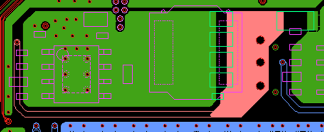
・1st layer's inductor and 8th layer's output capacitor are overlap (right behind).

・In general, in the case of 2 layer board have possible of noise.

⇒If 8 layer board and setting GND layer(2nd layer), noise problem is eliminate, is it correct?

Best regards,

Satoshi

  • Hi Satoshi,

    I think this layout could be fine if you could move the cap a little bit away from the inductor. In the buck layout, there are two concerns for the output power trace. The first is from SW node. The noise could be coupled via stray capacitance. The other is the eddy current from inductor. So try to keep away from these two parts for the output cap.

    For this design, the output positive trace start from inductor to the right to via and thru via to the bottom layer and back to the left to the output cap. For the ground layer, there will be no overlap part for this output positive trace. But since this trace do not carry high switching current, it is not critical for the EMI. 

    Best 

    Anthony