This thread has been locked.

If you have a related question, please click the "Ask a related question" button in the top right corner. The newly created question will be automatically linked to this question.

TPS54341 with Snubber Failing EN 300 440-1 clause 7.3

Other Parts Discussed in Thread: TPS54341

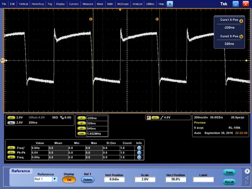
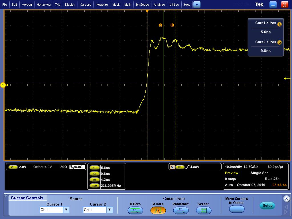
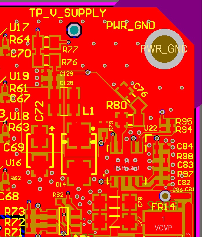
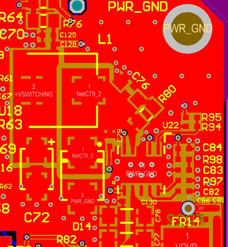
We failed ECE Reg 10 for Radiated Emissions in Europe by 4 dB @ 258 MHz. After probing around, most of the radiation was coming from the TPS54341 switcher. The solution was decreasing the DC switching frequency from 2.5 MHz to 2 MHz and adding a snubber. In the lab, this dropped the radiated emissions by 7 dB @ 258 MHz. Resending the boards for testing, they failed again, this time the test was EN 300 440-1 clause 7.3 and they failed by 9.2 dB @ 224 MHz. Has anyone else had trouble with the TPS54341 pass radiated emissions for EU? Does anyone have an idea how we can solve this?
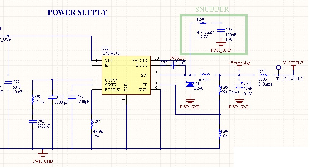
 

Setup for TPS54341:

Switching frequency: 2 MHz

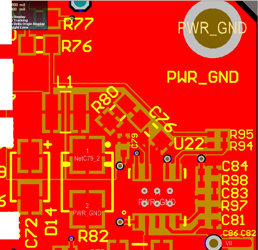
Snubber (placed before output unductor): 4.7 Ohms in series with 120 pF

Vin (average) = 12 V

Output Inductor: 6.8 uH (SRN3015-6R8M)

Output Cap (after output inductor): 47 uF

Other helpful information:

The unit passed FCC Part 15.209 @ lower emission testing

  • EMI testing is always done at the system level.  If you are having trouble wit radiated emissions, maybe you should consider a shielded enclosure.  You can also tune your snubber and switching frequency to avoid the frequencies where you are having trouble.  Poor layout can also contribute to EMI problems.  Can you post your schematic, pcb layout and a waveform of your switching node along with the frequency you are failing?

  • I don’t have any units to measure at the moment, but looking back at some previous waveforms I may have found one that represents the response we’re seeing out of the DC-DC converter.  The frequency it’s failing at is 224 MHz and it’s failing by 9.2 dB.

    Images:

    Schematic, layout, waveform

  • If that is supposed to be the SW node, it is rather unusual looking.

  • Yes, the wavefrom is the output of the SW node.
  • It appears to be a "reference" waveform rather than direct CH1. You should use DC coupling and zoom in a little further, maybe 20 nsec /div. You want to look at the ringing on the SW node at the top of the rising edge. Use full BW.
  • Yes, it's a saved waveform. I can't bring up a different waveform until we get more units. I noticed the ringing when we were seeing issues at 258 MHz, but haven't looked for the 224 MHz. I anticipate we'll see something there. Are you asking these questions because you don't think it's the DC-DC converter?
  • It could be something else, but high frequency noise in the 80 - 300 MHz range is commonly caused by switch node ringing. You have to match you frequency domain sweep to time domain waveform to be sure. If you don't see the frequency ring on your SW node, then you will need to look elsewhere.
  • Here's a picture of the switching noise without the snubber measured on the output of the DC-DC converter. Our oscilloscope measured it around 238 MHz.  It could be that our oscilloscope measurement is off slightly, but you can definitely see the small ripple at the higher frequency:

    What do you think of the layout? I went to the layout again and saw that there aren’t a lot of vias outside of the DC-DC converter, which leads to higher parasitic inductance to ground for the components that are outside the DC-DC converter (such as the snubber, diode, and C72).  Do you recommend more vias around components tied to ground?

    I believe I found the solution but I’m a bit skeptical of its reliability. It turns out if you change the snubber resistor to 0 Ohm and maximize Csnubber to something > 500 pF the noise we see @ 230 MHz goes down by 10 dB or more. However, I have yet to see a paper/article/post saying it’s OK to have Rsnubber=0. Is that something we can do?

  • Generally, if you have an internal GND plane, it is best to use a couple vias at the VIN and Vout capacitors to connect the returns to the internal GND plane.  Otherwise your layout looks generally pretty good.  I do have some concerns with the thermal reliefs.  Those thin traces may act as radiators.  As far as the snubber, the resistor is used to dissipate the power.  You might try going to just 1 ohm.  Enclosed is a paper that may help you optimize the snubber values.

    2260.RC Snubber.pdf

  • Hey John thanks for all the help you've provided so far, Preco really appreciates it. After reading the document you sent and through trial and error, I've optimized the snubber to further minimize the ripple we're seeing at 230 MHz. Now I'm using a 2 Ohm (1W) and 470pF (1kV) snubber - the low resistance helps minimize the 230 MHz ripple and the higher capacitor helps minimize the 230 MHz ripple at a higher input voltage (24V). Another improvement I saw was changing the boot cap from 0.1uF to 1uF, is that something I can do without potentially damaging the DC-DC converter?

    The image below is a picture of the new layout. I included more vias at the input and output and everywhere else for that matter. I also made the output copper area on the 'SW' pin larger because it sounded like from your previous response more area is better (and this tends to be a general rule of thumb). In order to make the area larger I brought the output node of the power divider to go through the power layer, will that have a negative impact on low frequency radiated emission we're seeing?  I also moved the snubber resistor close to the 'SW' pin because I found that when I measure the response on the 'SW' pin on the oscilloscope the ripple looks cleaner at the snubber than the response at the 'SW' pin and the output inductor pin 1.

    The optimized snubber managed to decrease the radiated emissions by 11 dB (average), which still isn't good enough. Do you think these new layout changes will further decrease the radiated emissions we're seeing at the output of the DC-DC converter? Is there anything you recommend on the layout or additional parts we can put on the board to help reduce the problems we're seeing? 

  • It is ok to rout the FB trace on another layer. I do that often. As far as the SW node copper, You generally want to make that area smaller not larger. But the most important thing is to not make it narrow. Even a short narrow trace will radiate more than a longer wider trace. I am thinking that your thermal reliefs may be an issue. We never use them. Otherwise the shape looks good. I would probably make the SW node copper smaller, but it does not look obviously too large. The other ting you could consider is some small value ceramic bypass capacitors on the input and output, 0.1 uF, 0.01 uf etc.

    We did not test with any other values of BOOT capacitor. We generally try to only recommend the suggested value. I do not see why 1 uF would help with EMI, but if it the difference between passing and failing, then I suppose it is ok. The main issue with larger BOOT capacitor is at start up. If the COMP pin rails out before the BOOT cap is charged above the UVLO, you will get a step on your Vout ramp up waveform. You can control that by holding EN low until the BOOT cap is charged, but you are using the internal UVLO on Vin.
  • Hello again John, this should be the last time I message you about this thread other than informing you whether or not we passed EN 300 440.

    Thanks for the advice about the BOOT cap, we'll stick with the recommended value 0.1uF, unless we need to use the 1uF to pass EN 300. 

    I took your advice on making the SW node shorter and wider. I also made the footprint larger for the inductor so we have more options. The footprint on the layout below (see image) is for the 744314650 (6.5µH Shielded Wirewound Inductor 6A 21.5 mOhm Nonstandard) part of the same inductor family used on the datasheet. I also managed to squeeze a 1uF and a 0.01uF at the output and a 0.1uF at the input.

    In the prior board rev (one I haven't shown you a picture of) there were no thermal relief pads on the output 'SW' node and after testing multiple boards I found it didn't help the radiated emission issue we're seeing @ 230MHz. In this new and hopefully final rev, I put wider thermal relief pads to compensate between manufacturing tolerances and potential radiation thermal reliefs may cause.

    If you could quickly look over this board layout and comment on your impression of it that would be great – this is the last one my company will do before we have to ship to customers.

    Thanks a TON

    Brad

  • I do not see any particular issue with it. The neck down of the GND copper pour gets a little narrow where it goes under the IC, but other than that I do not see anything.