Because of the Thanksgiving holiday in the U.S., TI E2E™ design support forum responses may be delayed from November 25 through December 2. Thank you for your patience.

This thread has been locked.

If you have a related question, please click the "Ask a related question" button in the top right corner. The newly created question will be automatically linked to this question.

Confusion with bq769x0 balancing

Other Parts Discussed in Thread: BQ78350, BQ76940, BQ76920

Hello,

Need to confirm a possible override setting for cell balancing:

For bq769x0, SLUSBK2E has CELLBAL1, CELLBAL2, CELLBAL3, showing

CELLBAL1: CB5 CB4 CB3 CB2 CB1

CELLBAL2: CB10 CB9 CB8 CB7 CB6

CELLBAL3: CB15 CB14 CB13 CB12 CB11


Q1: There is “AFE Cell Balancex” registers in “PF Status” of “flash data summary” of SLUUAN7A. So does bq78350 copy what is these three regs directly to bq769x0?


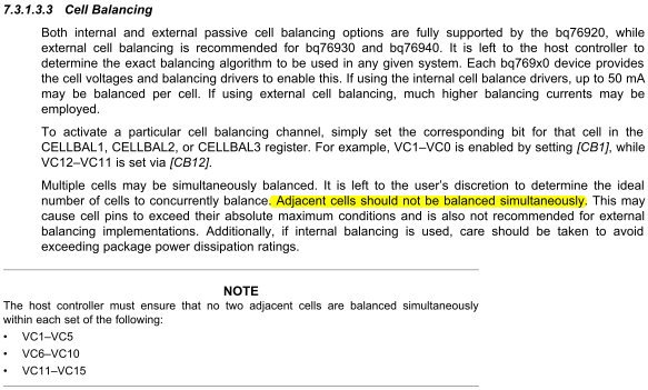
Q2: the DS also says adjacent cells should not be balanced simultaneously, further said the “adjacent” means within each 5-battery set as shown below. The expression is not clear enough. For example, according to “Table 8-3. Cell Connections for bq76940” there are many different mappings possible, and does the “adjacent” refer numbering of the actual cell, or of pins VCx?


Q3: Conflicts & Overrides:

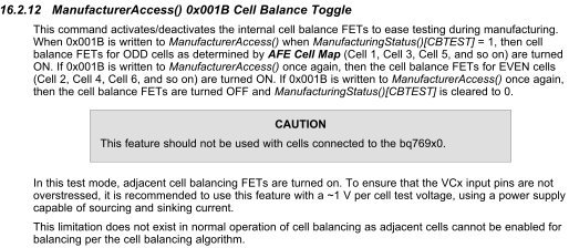
a)      ManufacturerAccess() 0x001B is said to temporarily enable balancing test. But the page also cautioned not to use with bq769x0. But bq78350 itself has no internal balancing FETs and actually is not DIRECTLY connected to the cells. What does this actually mean here?

Calino


  • Q1: From the construciton of the registers it would appear to be a direct copy of the AFE registers without reformatting.

    Q2: It is actually logical cells in the group which should not be balanced simultaneously.  When cell count is reduced those turn into physical cells also.  For example if a bq76920 is configured for 5 cells, cell 3 (VC3 - VC2) and cell 5 (VC5 - VC4) could be balanced simultaneously.  The voltage on cell 4 will approximately double which will be within pin limits.  If the part is configured for 4 cells, VC3 is shorted to VC4.  Actual or logical cells 3 and 4 can not be balanced because they are adjacent both logically and in physical connection: (VC5 - VC4) is now adjacent to (VC3 - VC2) since VC4 = VC3.

    If the part is configured for 3 cells, VC4, VC3 and VC2 are shorted.  If all 3 cells are at 4V and logical adjacent cells 2 and 3 are balanced, balancing pulls VC5 ~ VC4 and VC2 ~ VC1.  VC1 through VC5 would all be at ~ 8V which would violate abs max on VC1.  Other combinations of adjacent cell balancing can exceed differential voltage limits of the part.  When external balancing is used, the voltage across the common resistor in adjacent cell balancing will be approximately zero and the external FET will not activate. Adjacent cell balancing is not recommended.

    Q3: ManufacturerAccess() 0x001B Cell Balance Toggle command sends an alternating pattern to the balance control register and does not comprehend adjacent cells from the cell map.  So it could violate the adjacent cell balancing recommendation.  The caution is to not use the command with cells connected.  The next paragraph recommends ~ 1V per cell test voltage.  This would come from test equipment. If the alternating pattern balances adjacent cells, the low voltage should limit applied voltages to levels below the differential or single ended limits of the part.