This thread has been locked.

If you have a related question, please click the "Ask a related question" button in the top right corner. The newly created question will be automatically linked to this question.

UCC28700 Output Current Issue

Other Parts Discussed in Thread: UCC28700

Hello,


I am following reference design "http://www.ti.com/lit/df/slur930/slur930.pdf" 
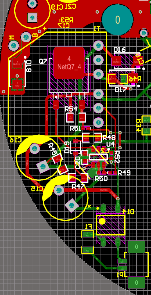
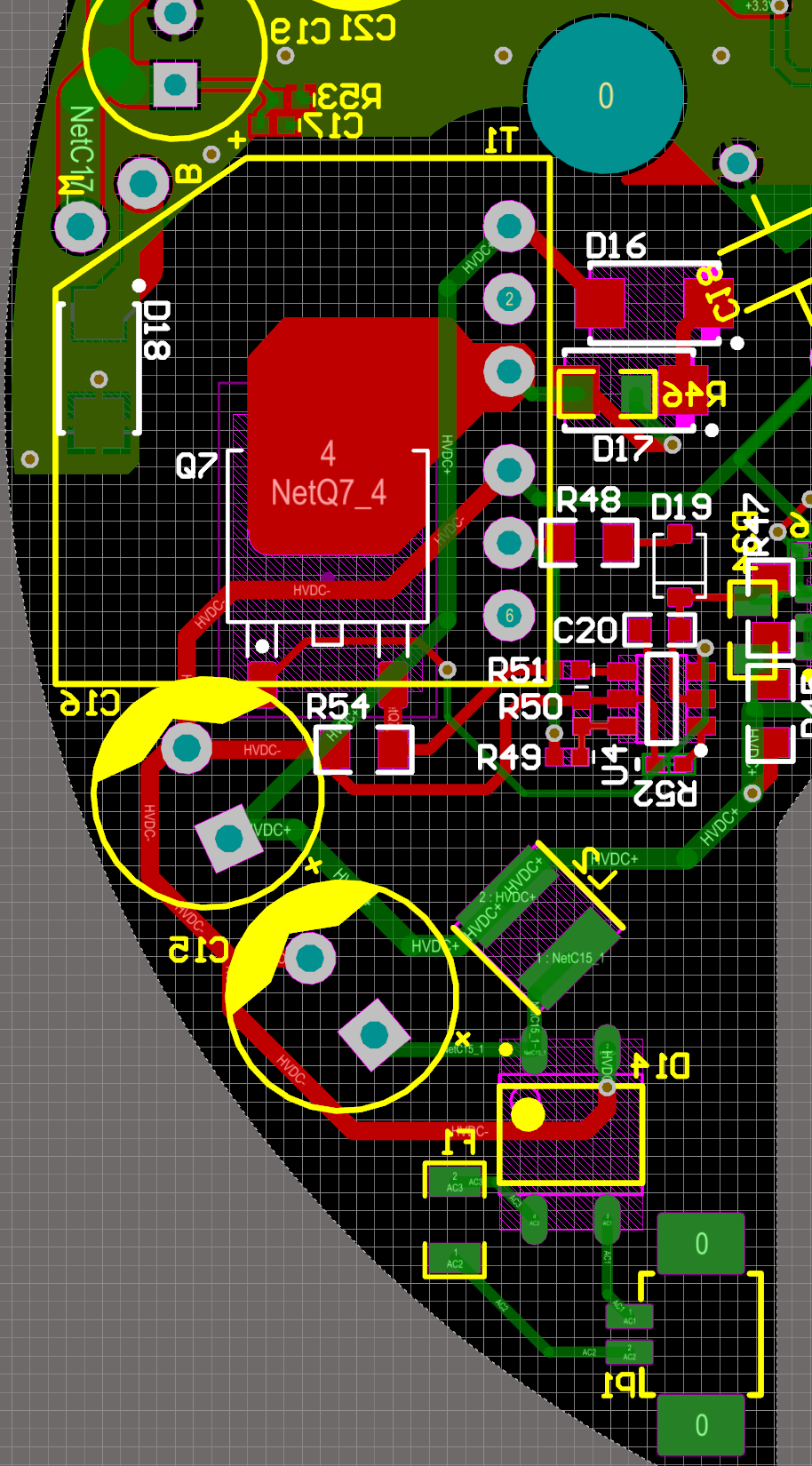
Attached is my schematic, I have changed Q7, D18, D19 from the reference design using similar components (D18 in mine is 5A, same voltage drop as in reference design, just smaller).

******EDIT******

Looks like my post was truncated. My issue is that my converter only works with extremely low loads, 0.4A max. The output voltage is ideal, 4.96VDC. I have tried changing the RLC from 3.01k to 1.5k, without any noticeable improvement. I suspect that it's a current sense issue, but I haven't used this sort of flyback regulator before so I'm in the dark here. Shematic attached.

  • Hi Zac,

    Not sure what your question is and also the schematic is not attached ?

    Regards

    Peter
  • Hello Zac,

    We'd like to help, but unfortunately your schematic drawing and your actual question or issue is not part of this posting. It's possible that the post was sent too soon while trying to attach the schematic file. Please repost with the missing information.
    Be sure to click on the "Use rich formatting" link at the bottom-right corner of the post box to enable the means for file attachment. After the formatting bar is displayed, click on the "paper-clip" icon to do the file attachment. The file will be inserted wherever the cursor is in your text.

    Regards,
    Ulrich
  • Original post edited, my schematic and issue were truncated or otherwise lost when posting.
  • Hello Zac,

    Based on your statement of "following reference design ...slur930.pdf", I assume that your design is essentially recreating the PMP8286 except without the USB chip and with 120Vac only input. Please correct me if I'm wrong.
    Based on this, I also assume you have your own pcb, not necessarily a 2-board cube, but probably a single board arrangement.

    The value of RLC is irrelevant for this issue. It merely adjusts the "tightness" of the current limit over min to max input line voltage range.
    There are 2 signals that can be influenced by noise: CS and VS, and of the 2, VS is more sensitive. Your board works up to about 20% of rated load, then doesn't work when increasing above that. I assume that it goes into a shutdown for some reason, then continuously cycles attempting to restart but can't stay running unless the load is adjusted to <20%.

    I surmise that there may be a noise interference issue with VS or CS (or both) based on the pcb layout. Spike noise on CS at higher loads could prematurely trigger pulse-by pulse shut down and result in this problem. Excess stray capacitance or distortion of the AUX winding knee-point can interfere with proper sensing of the waveform and mis-regulate or stop switching. One ironic aspect of this problem is that since it runs okay below 0.4A, it had to have started from 0V on the output, and the controller provides full power (up to the current limit) while charging the output caps from 0 to 5V.

    To see if it is noise on CS, I suggest to add a test filter cap of 100pF from CS to GND at the UCC28700 pins. This cap, not recommended for normal use, will suppress noise spikes if any and should allow the I-sense signal peak to rise higher and deliver more output power. (Note: The RC delay will increase the energy delivered per switching cycle, but this can be ignored for test purposes. You may have to increase the minimum load.) If successful, review your layout and components to find the source of the CS spikes.

    If the problem persists, look for noise or distortion of the waveform at VS. Leave the CS cap in place, just to keep any CS noise out of the picture. Using a normal scope probe on VS is generally not recommended because the probe capacitance itself can distort the knee-point being sensed. A low-capacitance probe can be used (< 5pF) but be aware that its 1-Meg resistance will alter the VS divider impedance and Vout will rise a little. A normal 10-Meg probe (10~15pF) might still "work" if it doesn't round off the waveform knee too much, although Vout will still change due to the different sampling voltage.

    Probing the Aux-winding waveform will not distort the VS signal, but you have to infer what that signal is by the divider. If the Vaux waveform has a lot of ringing during the demagnetization time that does not settle out, that can cause missed sampling and interfere with proper operation. This could be from stray inductance not clamped by the TVS.
    If probing VS, or placing a small cap <10pF on VS, seems to"Fix" the problem, then that is where to focus the debug and examine the layout for signal interference and noise coupling or excess area in the VS-sensing loop.
    Don't forget to ultimately remove the cap on the CS input, once the issue is resolved.

    Regards,
    Ulrich
  • Hi Ulrich,

    Thank you for your detailed reply. I will attempt to filter the noise with caps as you suggested. In the meantime, here is a picture of the layout (bottom view, red is bottom and green is top). Please let me know if you see anything terrible I've done. Thanks in advance.


  • Adding the 100pf cap on the CS line appears to have done the trick... highlighted below is the CS line. My thoughts are, 1. put the RLC next to the controller, and route the CS line on the right side instead of the left, shortening the distance and number of vias required. However, if my design always has a load on the 5v (it's not a USB charger), is there any real issue if I leave the 100pf cap on the line permanently?

  • Hello Zac,

    There are a number of changes that I would recommend for this layout, but a verbal description would be very cumbersome for me to write and for you to read and interpret. I can make some drawing markups but that'll take some time.
    However there is one thing that stands out to me: the L2 filter inductor is directly opposite the control IC and CS input. I suggest removing it temporarily and putting a shorting wire from C15 to C16 to see if that improves things.

    Your post about the 100pF cap on CS just came in while I'm typing this. I'll continue with this reply. I don't recommend keeping the CS cap, at least not as large as it is. It should be as small as possible to "fix" the noise, but ideally, a new layout can fix it and eliminate the cap. This is because adding a cap doesn't guarantee the margin to the extent of the noise, which may be less or more on other boards as component properties vary. Better to eliminate the source of the noise if you can than try to muffle it.
    Having a cap on CS creates an RC delay for the Ipk sensing which alters the operating points along the control law curve and raises the maximum current limit. A small value can probably be ignored, but a long delay slows response to an overload condition which may overstress other components. Minimize it or eliminate it if you can.

    Besides the location of L2 (which could be moved to the space just above bridge D1), the GND feed to the controller should ideally follow the R48/D19/C20 path, not come from the D1 - pin. There are other loops that can also be reduced, but these two changes may have the biggest impacts. Of course, if you make any layout change at all, you may as well make all beneficial changes that can be identified, and that is a significant task to detail.
    In a nutshell, loops to minimize include:
    a) Xfmr primary/Q7/R54/C16 loop
    b) Xfmr Aux/R48/D19/C20 loop
    c) CS path R54/R51/CS pin/U4-GNd/R54 loop

    Check out the above debug ideas, and based on the results we'll take it from there.

    Regards,
    Ulrich
  • I will test shorting L2 and see if the EMF from that was causing issues. I have created a new layout, where I have moved U4 away from noisy components. I have also shortened the CS and VS paths greatly, as well as kept them out of the noisy paths (exception being the gate drive between U4 and Q7 crosses over them both, but still 61mil away). I have also more directly fed R54 and U4 GND from C16, and L2 is further away from U4 and the CS/VS paths. Your thoughts?

  • Hello Zac,

    I agree, I think this is an improved layout and should preform better than your earlier one. I do suggest one thing: to disconnect the HVDC- track from R50 and run it straight across from R54 to R52. This will reduce the loop area for the gate-drive current, which has a high di/dt at turn-off. That should help cut down on radiated noise. Compared to the gate turn-off edge, the other signals are slower and bigger loops there will have less of an impact.

    The CS signal loop becomes a bit wider, but the gate-turn-off happens after the CS signal has reached the turn-off threshold, so the turn-off di/dt will not affect the CS signal. You can reduce the CS loop a bit by making the track from R54 to R51 more of a right-angle and closing up the area.

    Good luck with your new layout. I hope it works out well.

    Regards,
    Ulrich
  • Hi Ulrich,


    Thank you, again, for the detailed help. Here's the final layout, taking into account your last recommendations. I have moved R54 closer to R51 in order to shorten the CS path, and supplied HVDC- to U4 via R52.

  • Hi Zac,
    Yes, that looks pretty good. I'd say it's time to fabricate a new board and test it out.
    Regards,
    Ulrich