A related question is a question created from another question. When the related question is created, it will be automatically linked to the original question.
If you have a related question, please click the "Ask a related question" button in the top right corner. The newly created question will be automatically linked to this question.
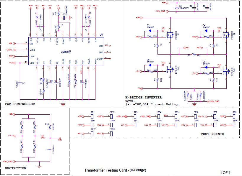
Regarding LM5045 - pulses are not generating from the HO1, HO2, LO1 & LO2
The Input voltage is only about 28V dc. As you can see in the schematic as +28V net name. The Voltage across REF is getting as +5V, UVLO Voltage is around 2.5V and OVP Voltage is around 640mV. But Unable to check pulses(no switching,i.e., 0V) to mosfet
Initially, I do not see anything wrong on your schematic - althoogh the resolution is not so godd, it's hard to read some of the values.
I assume that you have checked your board for faults, sharts, opens etc, esp around the pins of the LM5045?
I would recommend checking the voltage levels and waveforms on some key pins.
- VCC - should regulate at ~ 9.6 V after startup
- SS - at power-up, this pin should ramp up to ~ 5V - with 22 nF cap and 20 uS charging current, it should ramp about 900 mV every ms.
- COMP - check this together with SS - COMP should follow and track the rise in SS at startup - once SS has charged up, COMP should sit at ~5 V, since it seems to be configured open-loop in your schematic
- RAMP/SLOPE pins - these should show a low-level ramp signal from the 100 uA current source into the 1-k-ohm resistor - however, I now see that the Rfilter resistor from the CS shunt is huge - 47 k-ohm. This is probably causing your issue. This will develop far too much voltage across it from the SLOPE 100 uA current source. Also the CS filter RC time constant is far too long, 15 us, for Fosc ~1 MHz. I would recommend dropping the 47 k-ohm to 470 ohm or less.
Yes, I checked VCC its coming as 9.6V intially, when I am below Vin =13Vdc (Under-Voltage = 13.75V & Over-Voltage = 58V). As I am increasing the Vin above 14V, VCC get dropping to 7V. However the gate pulses are generating with minimum duty ratio and I am unable to change the duty ratio of Pulses. As per schematic I didn't load VCC. Can you suggest me to overcome this issue?
As I mentioned above, the resistor RF1 feeding the CS pin is far too large - this will set a high-amplitude slope comp ramp signal on the cS pin which will terminated the gate pulses very early, as you are observing.
Try changing RF1 to ~470 ohm or similar, and see if this helps.


