This thread has been locked.

If you have a related question, please click the "Ask a related question" button in the top right corner. The newly created question will be automatically linked to this question.

TPS54331 not working continues

Other Parts Discussed in Thread: TPS54331

Hi

im working on 24v-5v DC-DC converter with TPS54331 but i have problem :

1-after about 3 hours TPS54331 SHUTDOWN and i dont have 5V output and i measure the EN pin voltage its about 200-900mV and its below 1.25V .

i reset my input and output drop from 5V and its flashy and i see some little spark on 384k resistor(all of my resistor are 0805)

2-when i disconnect the EN voltage divider ,the EN pin voltage is about 4.5V and after 5 min TPS54331 SHUTDOWN!

i do all of this without load 

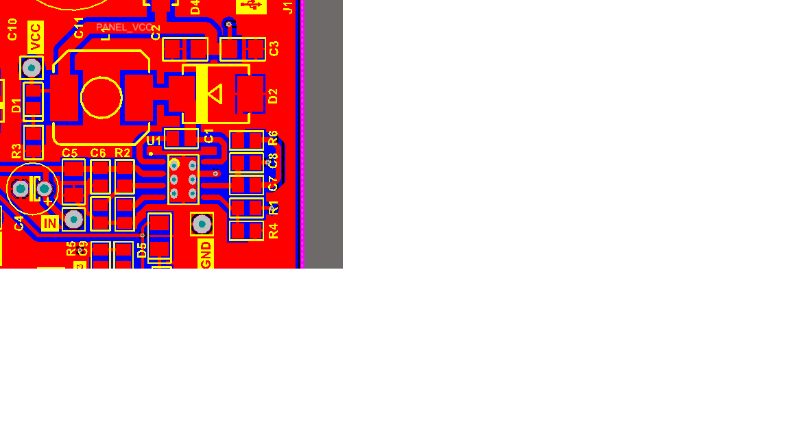
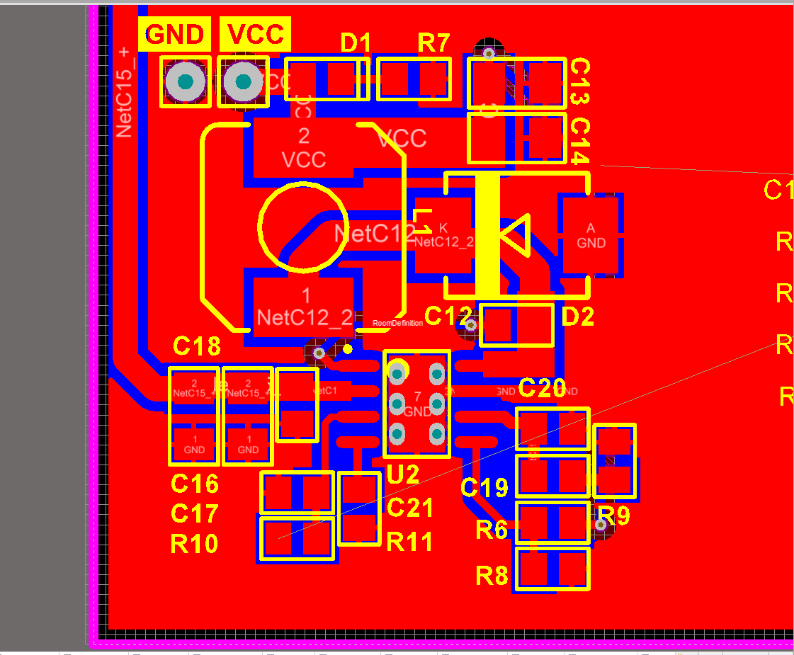
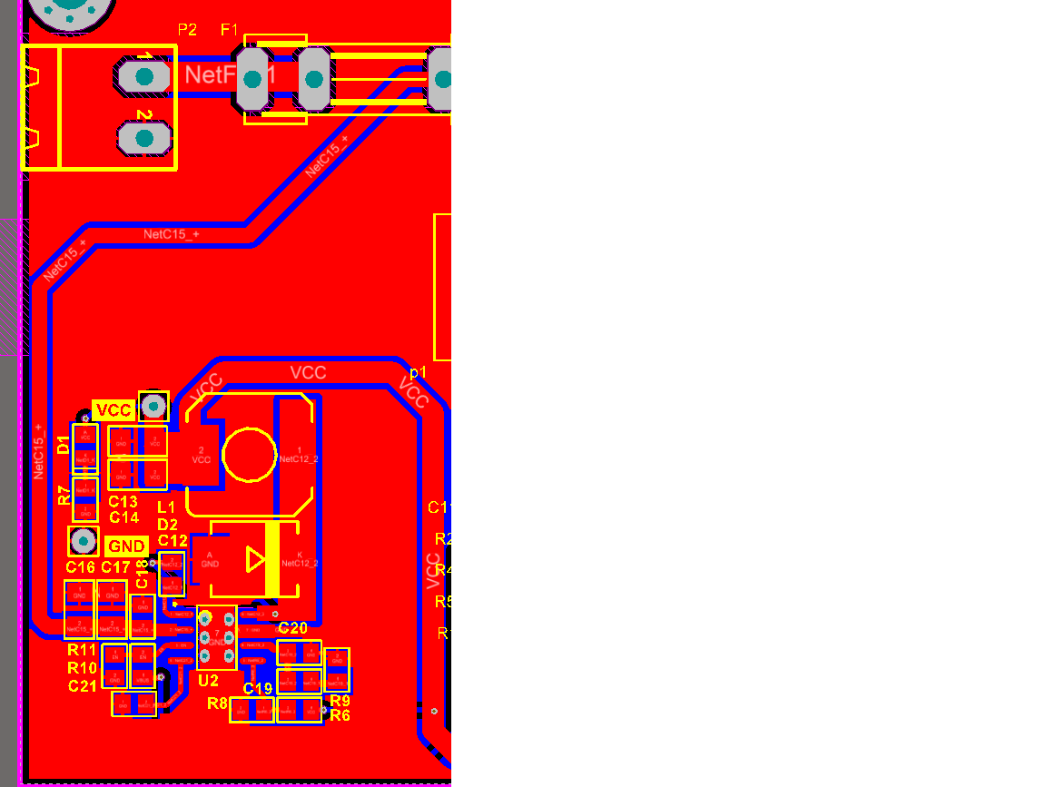
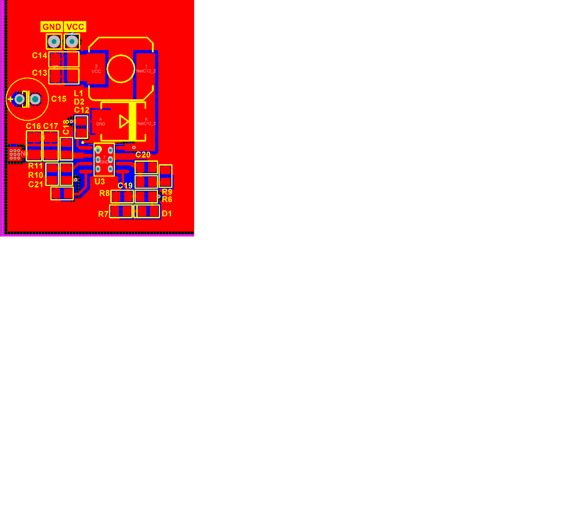
here is my schematic

  • What do you mean by "flashy"? Your schematic seems ok. Can you post your pcb layout? Ans some waveforms during normal operation including the PH pin and VIN?
  • Hi John
    Thanks for your reply
    it means sometimes its turn on and sometimes its shutdown ...

    (i use 1.8k and 390 ohm Resistor for EN pin but the 1.8k Resistor heated alot that burns my finger!)

    here is my PCB layout:

  • Those EN resistor values seem extremely low.  Try Rtop = 169k and Rbot = 32.4 k.  Your layout looks like it has issues as well.  The input caps should be closer to pin 2.  Move the EN resistors away.   The ground path at the catch diode is blocked by the BOOT resistor.  Even though it seems like a "direct connect" from pin 8 to pin 1, don't do that.  Leave a fat top side ground trace there and use a via to connect the BOOT cap on one end.

    All that being said, you may have damaged the IC.  You should probably replace it.

  • Hi john
    thanks for your reply, so you said my strange behavior is because of this 3 steps?
    is ground plane really important link this?!
    and could you please explain about "Even though it seems like a "direct connect" from pin 8 to pin 1, don't do that."
    What do you mean by "direct connect"?
  • I cannot be 100% certain, but those were things that I noticed that could affect your design. The direct connect comment is that it looks easy to place the BOOT capacitor directly between pin 1 and pin 8 and connect both ends. But then you do not have easy access to the pin 7 GND. You return current from the catch diode must go all the way around the IC. You definitely want to minimize that distance.
  • Hi

    This is my new Design and i try to consider john's tips.

    How is this?

    (one of the net is for EN pin because i want to turn TPS54331 on/off with another signal in my design)

  • Generally that looks better. I would flip the catch diode and inductor horizontally to minimize the SW node and GND paths. You can rotate the inductor 90 deg so the SW node pads are directly adjacent. You can route GND path under the IC. Flip the input caps vertically and route to GND at the top of the IC as well. See the datasheet layout guideline and look at the EVM users guide layout. The EVM layout could be improved by moving the L1 and D1 to the right so the D1 GND pad is directly above the IC, making the most direct GND and SW node paths. Finally, get rid of the 2 thin (thermal relief?) traces at the exposed pad under the IC.
  •  Hi john

    This is my Final Design i looked at EVM board and Layout Guidelines.

    I rotate SW component on top of the ic and now i have clean direct GND path .

    How is this?is it professional ? :)

    (i should be worry about final size of this module on my PCB)

  • Hi john
    could you please look at my design if there is any layout problem?
  • That looks good except you still have the thin traces from the thermal pad to the main copper pours. Can you make that a solid fill or increase the number of traces?
  • Hi 

    thank you john for your reply ..without your help i cant dont that.

    this is the other design .but i have some question:

    my current PCB as i say it dosent works well(its flashy and ...)why it dosent work?does it matter to catch diode placement in my PCB and layout problem ?i change my IC two times but it dosent works!

    2-i use via to connect cap on BOOT and PH pad ,but the PH pad is on bottom layer .is this cap important and the placement is necessary ?

    3-as you see in picture i have 3 polygan part on top layer (there is no polygon on right side) and im worry about ground path because the input conector is on left ,top the board and the GND polygan does NOT direct connect to TPS54331 circuit (should i use via on top of the tps54331 circuit?)

    thanks

  • 1.  I suspect your underlying cause is probably the choice of EN resistors.  But it is very important to have a good PCB layout as well.  Did you try the EN values I recommended?

    2.  It ok to use that method for BOOT cap connection.  That is how I do it.

    3.  I se your point here.  You will have to find some way to directly connect your input GND to the IC GND.  You could move everything over to the right and place the GND connection adjacent to the VIN path (and maybe widen VIN a little as well).  Or route it on the bottom side (which I assume is mostly a GND plane anyway?).

  • Hi
    i change the EN resistor to those value that you say but still it doesnt works!!
    i think one of the most important reason that its not working because of the GND and catch
    diode GND path .... is it really important that cause my circuit not working!?
  • Yes layout is vital. I checked your EN level with 1.8k and 390 ohm EN resistors and got 7.017 V start and 7.012 V stop...too close together. With 24 V in you should still only have about 11 mA, not enough to get the resistors hot and the voltage will be 4.27 V on EN, below the abs max There must be a fault somewhere. When you get your new board ready, we can look at some waveforms to see what is going on with it.
  • Hi john

    this is some waveform of my circuit that has problem(flashy!)

    i have something like this on PH  pin BOOT pin 

    and this is my EN pin:

    im confused! i just have a voltage divider on EN pin but its 1.4v!!! and my input is 24v

  • EN should be around 4.27 V. with 1800 and 390 or about 3.86 V with the values I suggested.You must have a fault somewhere. Either you are damaging the IC or there is some external fault for you to find. You will need to find this before proceeding further.
  • Hello

    I test my pcb for about 6 days its OK but after it the tps54331 seems not stable and its turn on and off randomly...i check my circuit many times and there is just one thing that is notice and thats it : the 100nF capacitor between PH and BOOT pin, i dont know that is X7R or not but i think its regular capacitor (its not x7r or x5r),could this be the cause of that strange problem?

    know i replace that cap with x7r and the circuit works fine for 2 days.but i want solve this problem forever.

    thank you

  • You definitely need a quality dielectric ceramic capacitor for the BOOT cap.  But your issue could be any number of things.  How did you determine the component values used?  Can you post your schematic along with your operating conditions?  Did you follow the layout guidelines?  PCB layout is critical for proper operation of dc/dc switching regulators.  Are you using the DDA package with thermal pad?  Is it soldered down correctly?  Did you check all the other components for proper installation and soldering?  Can you post waveforms of the unstable operation?  be sure to include the PH node.

  • Hi 

    these are my schematic and my layout.the

    vin=19.5v,

    vout =5v,

    Iout=appr. 200mA

    when its not working i think the mosfet is turn off!because idont have any output!

    i have led indicator for output voltage thats flashy!!

  • flashy.rar

    this is video of the flashy state of the circuit when the boot cap was regular(i dont replace it with X7R one).

  • I don't see anything that jumps out at me for the schematic or layout. I'll have to see waveforms.
  • Hi john 

    could you see my video?

    thanks

  • That is just a video of your board. I can't tell anything from hat. I need to see actual operating waveforms.