This thread has been locked.

If you have a related question, please click the "Ask a related question" button in the top right corner. The newly created question will be automatically linked to this question.

TPS65721 large difference on power dissipation while switching from DC-DC PFM to PWM.

Other Parts Discussed in Thread: TPS65721

We have 2 questions:

1) We see a large power dissipation jump from PFM to PWM, about 100mA in operation mode. What`s value that we shall see. Seems its too large.

On the data sheet (TPS65720m TPS657201m TPS657202, TPS65721), the quiescent supply current I_Q on chapter 7.5 (Electrical characteristics) is 2.8mA vs 36uA, what`s the operational case?

2) The transition happens at around 40mA. what`s value that we shall see. 

In addition, we have SYS to power up LDO instead of using DC-DC line. We use LDO to feed a PWM generator chip which draw power from DC-DC line.

  • Hi Zhonghua,

    1) How are you testing this dissipation current vs. power consumption from the DCDC loads?

    2) The transition from PWM mode to PFM mode occurs once the inductor current becomes zero in the Low Side MOSFET, so it ultimately depends on the external components. It will convert back to PWM once the required load current can no longer be supported with this PFM methodology.

  • Hi, Richard

    Thanks a lot!, Here is what we found

    PMIC chip: tps65721

    Issue: large current draw (>100mA delta) while switching from PFM to PWM on DC-DC lead

    Testing setup:

    1. No load on DC-DC output
    2. We have a meter to measure the current draw on input voltage pin (V_AC)
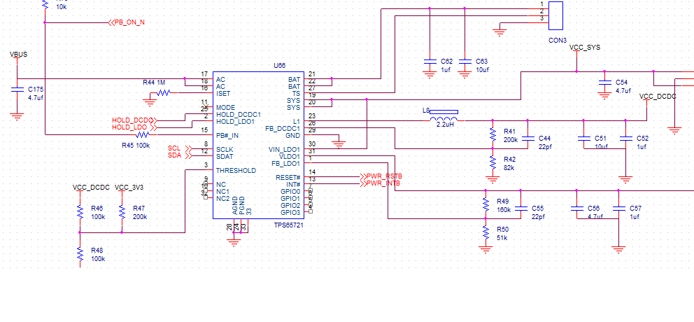
    3. We have another meter to measure the voltage drop on the inductor (L8) at the DCDC output L1

    Testing procedure:

    1. The chip is at PFM mode after powered up, and we measure the current draw on V_AC
    2. We forced the chip to work under PWM mode by pulling MODE pin to high, and we monitored the current draw change on (setup2) and check the voltage drop on (setup3).

    What is observed:

    1. We notice there is around 100mA difference. The value can be a little random. It could be 120mA high.
    2. There is almost no voltage drop observed on (Setup3) during the procedure, and It was concluded no load on the downstream circuitry.

     So It`s concluded that the current dissipation is within tps65721, but it`s so large that we don`t know why. Our schematics is attached, basically follow your reference.

    Again, Thanks a lot for your help. 

  • Hi Zhonghua,

    Doing the same test on an EVM showed the power supply jump from 1mA to 6mA when moving from PSM to PWM mode with no loads, so this is not specific to the part itself. Are you seeing this on multiple units or just one?
  • Hi, Richard

    Yes, The above is consistent on all the boards that we have. Have you seen any other people to report the similar issues?

    Thanks a lot!
  • Hi Zhonghua,

    No I haven't heard of similar issues, 100-120mA is a fairly large increase in current consumption and is unexpected.

    Do you see any changes on BAT or SYS during your testing? Could they be drawing increased current?
    Do you see the same behavior when you remove R46?
    Does the current increase similarly when using i2c to force PWM instead of the MODE pin?
  • Hi, Richard

    Thanks. We located a board (different batch but using same schematics) with different result. The board shows 15mA delta on V_IN while switching from PFM to PWM

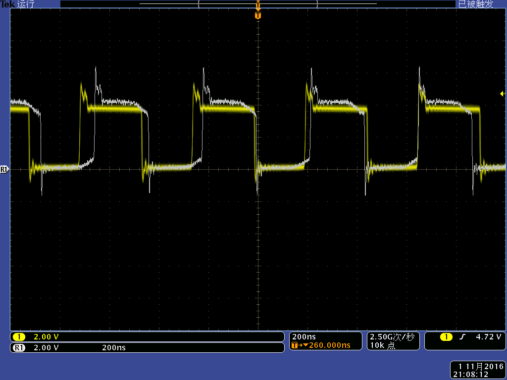
    We measure the voltage before the conductor (L8), though there seems no much difference. The yellow curve is from the boards with 120mA diff from PFM to PWM, the white curve is from the board with 15mA from PFM to PWM. 

    and

    1) we don`t see current on SYS, we will verify the BAT (though BAT is not connected).

    2) we will check and get back to you.

    3) Yes, we tried both.

    Again, Thanks a lot for your help

    Zhonghua (Joshua)

  • Hi Zonghua,

    I'm assuming both boards have identical voltage dividers for DCDC1, and same conditions such as input and output voltage, correct?

    If the two boards have seen different hours of operation it could be an indicator of electrical overstress, can you identify if the 15mA board starts to see an increase in current consumption over time? What feeds VCC_3V3 in this design and is it necessary that a path exists to DCDC1 via the threshold pin?