This thread has been locked.

If you have a related question, please click the "Ask a related question" button in the top right corner. The newly created question will be automatically linked to this question.

TPS65023B DEFLDO[2..1] pins issue

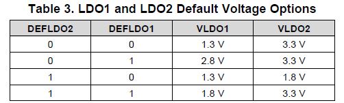
8.5.1.1 DEFLDO1 and DEFLDO2
These two pins are used to set the default output voltage of the two 200-mA LDOs. The digital value applied to
the pins is latched during power up and determines the initial output voltage according to Table 3. The voltage of
both LDOs can be changed during operation with the I2C interface as described in the interface description.

DEFLDO1 & DEFLDO2 latched during power up timing limited?

Current circuit: VIN:5V to DCDC2 output 3.3V to DEFLDO2, DEFLDO1 to GND. When the power up, the VLDO2 output is always at 3.3V.


  • Hello Eric Lo63813,

    Ok so going through your circuit, it seems you are enabling the LDOs at the same time as the Bucks. So when the LDOs are starting up initially it is reading in LOW for both DEFLDO2 and DEFLDO1 pins before the output of DCDC2 gets to DEFLDO2. That is why VLDO2 outputs 3.3V when powering up since you are meeting the first option.

    So for the desired output of VLDO1 = 1.3V and VLDO2 = 1.8V. Try tying DEFLDO2 to Vcc that way on start up it is reading DEFLDO2 as HIGH and DEFLDO1 as LOW. If you need the LDOs to turn on after DCDC2, try using DCDC2 to enable the LDOs.

    Hope that helps!

    Albert Lo