This thread has been locked.

If you have a related question, please click the "Ask a related question" button in the top right corner. The newly created question will be automatically linked to this question.

BQ76PL455A-Q1 I can't read analog values

Other Parts Discussed in Thread: BQ76PL455A-Q1

Hi, I am using BQ76PL455A-Q1 to develop a BMS
I encounter the following problem, when you perform any reading through the command register, only receive the digital die temperature. I have set the BQ according bq76PL455A-Q1 Reference Design Software.
What could be the problem?

Thank you very much.

  • Can you please explain how you are sending the command, through the GUI or via host MCU?

    What is the exact command (frame bytes) you are sending?

    How have you configured the CHANNELS register? Or is it still set to the factory default value (0xFFFF)?

  • I send and receive the content of the register, so that communication is correct. In fact, I receive a data frame with the appropriate length depending on the selected CHANNEL REGISTER channels, and correctly receive the value of the digital die temperature in the corresponding position according to the selected channels. I have in the written record FFFF03C0 (CHANNEL REGISTER). The frame bytes that shipping is 9403ffff3c0914d.
  • Can you please share the sample command frame that you are sending, along with the response frame received?
  • I send 81020295C, now I have in the CHANNEL REGISTER (000001C0) Only AUX0, Digital Die Temperature, Analog Die Temperature, I received (0500007E9600 and CRC).
  • Please confirm that the sample command you are sending is 0x81000200295C?

    It seems like you are missing 2 zeroes in your response frame. Can you please verify that you are receiving 0500007E9600CRC or 0500007E960000CRC?

    The first measurement is AUX0 (0x0000), followed by the digital die temp (0x7E96), then the analog die temp (0x0000). I'm not sure why you are reading 0V. I see a value here when I use the EVM.

    Are you using the EVM or your own board? It appears this may be a bq76PL455A-Q1 implemented as a communications bridge, so VM, CHP, CHM and OUT pins left un-connected. These pins will need to be connected to measure the analog die temp and AUX inputs.

    Please share more details of the application.
  • I send 0x81000200295C, I received 0500007E960000CRC. I'm using my own board to Which it's supply externally 5V supply in VP and VDIG, and 3.3V in VIO.
    OUT1 and OUT2 Have a capacitor of 0.1uF. I'm un-connected pin TOP, and now I disconnect cells, it is necessary to connect a minimum of 4 cells to supply the Bq76pl455A-Q1 through pin TOP?
  • Please share the schematic... It sounds like you have not connected everything correctly. Just from what you've explained, you are using the device in a way that is unsupported. For example, we only support powering the device from the external NPN circuit. bq76PL455A-Q1 is designed to control its own VP/VDIG supply. Top must also be connected to the highest cell, and must be 12V minimum. The OUT cap value is recommended to be 390pF with our recommended ADC settings.
  • I modify register 14 to allow external supply, 

    Can be supplied TOP pin  without being using voltage regulation (Pin NPN)?
    The other external components are the same as in the datasheet.
    I modified the sampling configuration to 99.92us. I have tried all the possibilities for sampling.

  • Please download the latest version of the datasheet, which has some updates to the sections you are referring to.

    That note does state that VP can be supplied externally, however, there is no recommended schematic provided for that use case.

    You still haven't shared a schematic, so I really can't give you all the guidance you need for your particular application. If you are connecting cells, TOP must always be connected to the highest cell with the circuit shown (C21, D5, D6). Please also ensure that VP/VDIG power is removed while the device is in shutdown mode, or there may be excessive current consumption.

    The OUT cap may be shown as 0.1uF in that particular diagram, but the 390pF value is described in several places throughout the datasheet where recommended ADC settings are provided for best accuracy.

    You may have damaged the device by not connecting the TOP pin, due to overstress of the internal ESD structures.

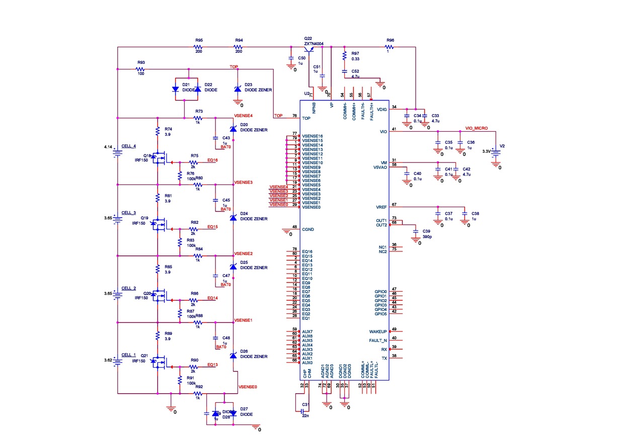
  • This is the actual schematic.TX,RX and Wake-up is connected to micro.

  • I see some mistakes in this design:

    • R93 needs to be a value from 100 - 300ohm only. A 1k value here could cause damage to the internal ESD structures in the device. This is described in the 2nd paragraph in section 8.1.1.3 of the datasheet.
    • The device requires TOP to be connected, and you have that here, however, the device supports a minimum of 12V on the TOP input. With just 4 cells, the cells will only need to be at 3V to be below the minimum operating limit for the device. 
    • The highest connected VSENSE channel needs to be connected to all the higher unused VSENSE inputs. Currently it looks like VSENSE5 - 16 are connected to each other but not to VSENSE4.
    • The balance FETs are connected to the wrong EQ pins. The gate of the balance FET for cell 1 should be connected to EQ1, not EQ13 as shown, The same problem exists for all other channels. The EQ pin is driven based on the voltage present between the 2 VSENSE pins corresponding to that channel. By connecting high EQ pins to the lowest cell channels (e.g. EQ13 to the cell 11 balance FET), it is possible that you have damaged the device.
    • If VP is supplied externally, it should be turned off when the device is in shutdown mode, otherwise there may be excessive current consumption. This is described in the 4th paragraph in section 7.4.1 of the datasheet.
    • The bottom of cell 1 should be connected to GND.
    • C33 should be 4.7uF
    • Can you please confirm the value of the balance resistor? It appears to be 3.9ohm. If so, that is really high for a passive balance design, and I hope you have designed the board to be able to cope with over 1A of balance current. 

  • This is the actual design, I supply with transistor.I modified according to its previous recommendations. In VP and VDIG, there are 5.33V, but when the BQ76PL455A-Q1 communicates VP fall to 4.78V. the above problem persists.

    Thank you for your attention.

  • I would try to replace R64 and R66 to a sum of ~100ohm, so maybe just 100ohm and ohm or 2x 50ohm.

    The following problems are still there:

    • The highest connected VSENSE channel needs to be connected to all the higher unused VSENSE inputs. Currently it looks like VSENSE5 - 16 are connected to each other but not to VSENSE4.
    • The balance FETs are connected to the wrong EQ pins. The gate of the balance FET for cell 1 should be connected to EQ1, not EQ13 as shown, The same problem exists for all other channels. The EQ pin is driven based on the voltage present between the 2 VSENSE pins corresponding to that channel. By connecting high EQ pins to the lowest cell channels (e.g. EQ13 to the cell 11 balance FET), it is possible that you have damaged the device.
    • Can you please confirm the value of the balance resistor? It appears to be 3.9ohm. If so, that is really high for a passive balance design, and I hope you have designed the board to be able to cope with over 1A of balance current.

    Like, I've said, I think you may have damaged the bq76PL455A-Q1 by not connecting it correctly.

  • Sorry for the schematic, but EQ are not yet connected, they have not been connected, because they have not yet been used. VSENSE4 is connected to VSENSE 5 (though in the schematic is not). What could be the underlying cause that can receive digital die temperature, but no measures analog?
    Sorry for the disturbances.
  • I can measure both with the EVM, as I've described earlier.

    Can you please confirm that the IC has always been connected properly, or was it connected incorrectly at some point in the past? If you are saying that the latest schematic you've shown (plus VSENSE4 connected to VSENSE5 and EQ not connected) is how the device has ALWAYS been used, then I can't say why you are not getting the correct response. If you've been modifying the connections based on feedback, and the same device was previously not correctly connected, then you may have damaged the device.

    Have you tried reducing the values of R64 and R66 to sum ~100ohm?
  • After changing the device Bq76pl455a-Q1, I can read analog values, but Vsense_2, and Vsense_4 give very oscillating values, which can get to oscillate 1V. I have only 4 cells, (15V among all). The other Vsense entries work correctly.