This thread has been locked.

If you have a related question, please click the "Ask a related question" button in the top right corner. The newly created question will be automatically linked to this question.

UCC28631 not starting up

Other Parts Discussed in Thread: UCC28631, UCC28633, UCC28630, LM2623

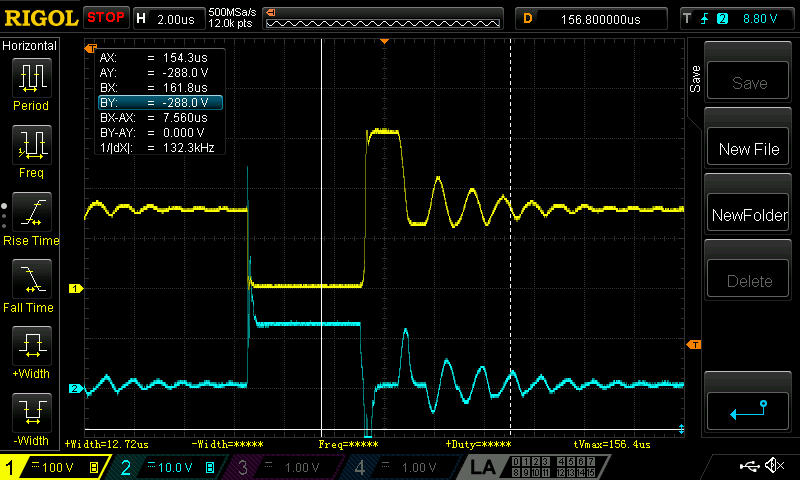
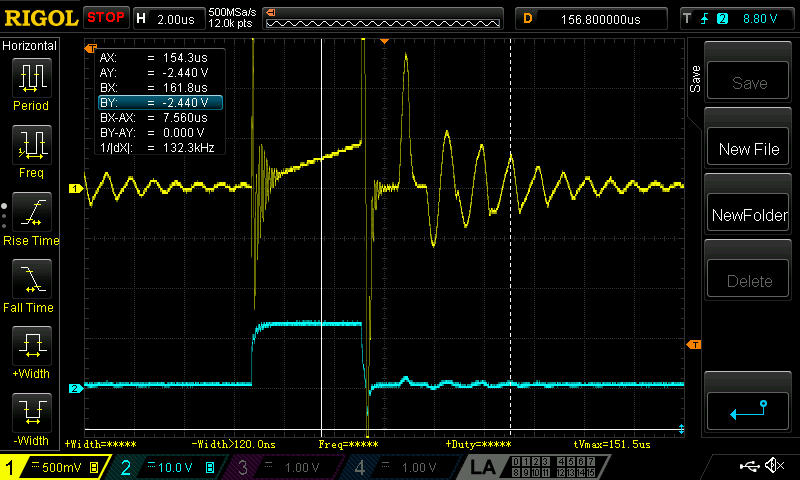
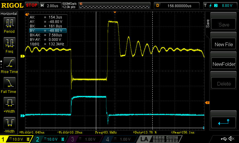
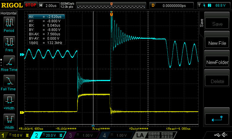
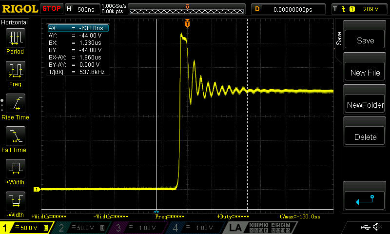
I have a 550uH 8:1:1 transformer with 10% max leakage, Rp=3.92K, Ra=24.3K, Rb=47.5K and Rcs=0.4

output target is 12-15V (not picky since it replaces an unreg supply) at 36W (also not critical)

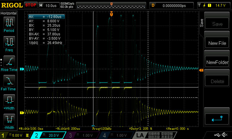
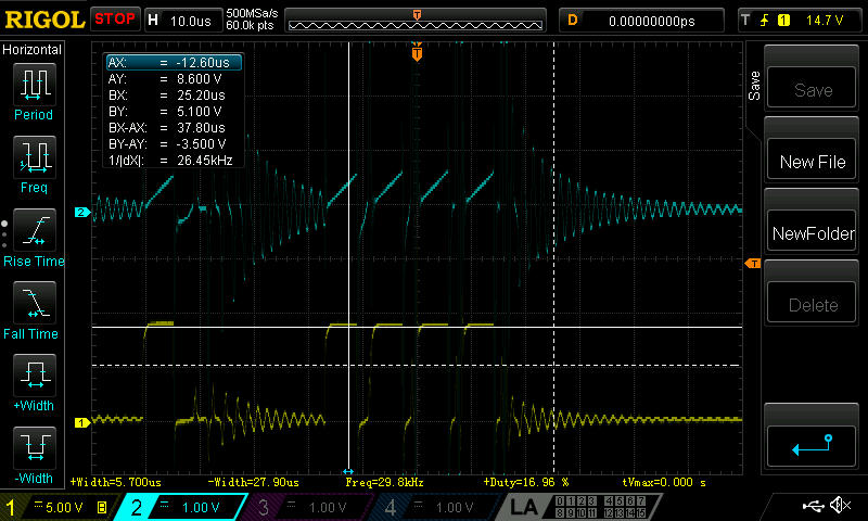
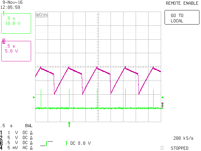
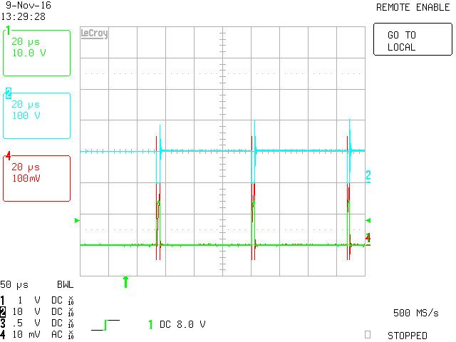
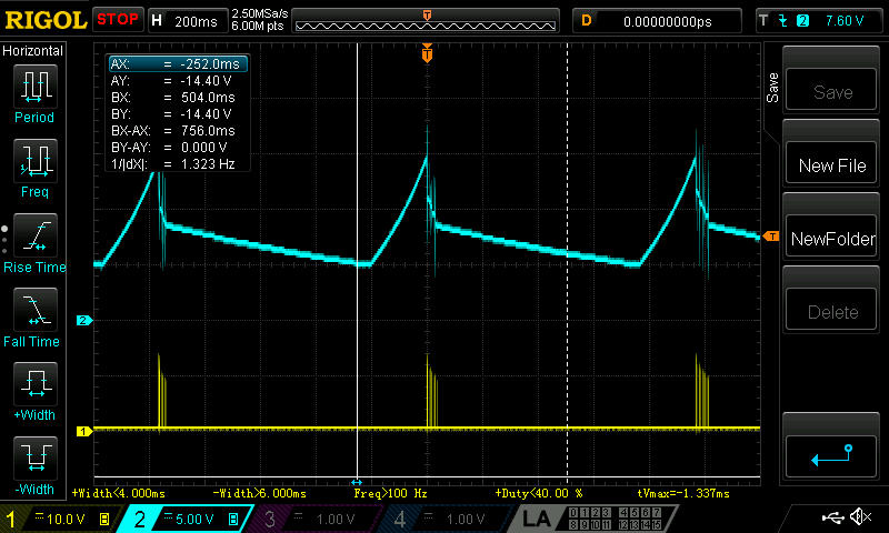
the chip error code varies between VDD low and Vbus low at 150V bus under no and low load

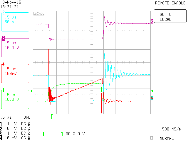
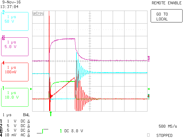
seems like the only things amiss from the forums is bringing it up slow and a standard RC clamper

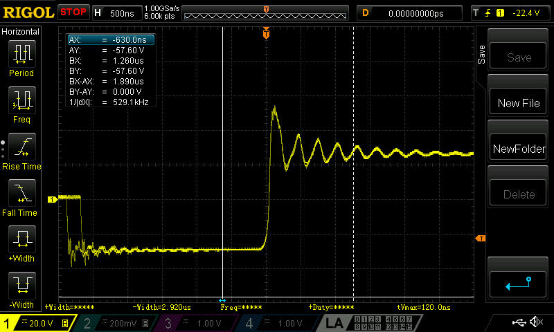
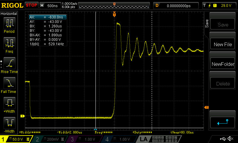
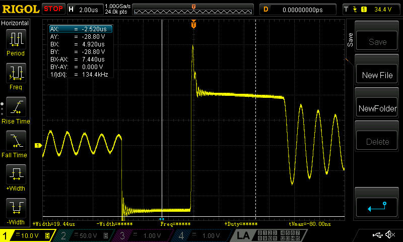
any thoughts while i try to rig a 200V clamp?

  • Dan,

    Can you post your schematic, Excel design calculator (if used), and some waveforms? In particular, what output preload resistance are you using (provides the necessary minimum load when external load is zero), and what series resistance do you have in series with the bias rectifier diode?

    Are you saying that it does not start up at all?

    Or cannot start under light-load or no-load?

    Or cannot stay running under light-load or no-load?

    Can you get it to start and run under some or any line/load combination?


    If you can provide some more details about what's happening, it will be helpful.

    Thanks,
    Bernard
  • does not start at all.... not at low line, not at rated line, not at no load, not at light load ( 200 ohm )

    buzzes at around 100hz sometimes and quits ... error codes either low vdd or low hv ... (those codes should be on the data sheet: makes a lot more sense when you know why it does not start)

    4.7ohm in series with the bias and 10k that needs to be reduced to 5k or so for the load....

    either i am missing something stupid or my ad blocker is preventing me from posting the schematic
  • just downloaded the xls ... does not seem to mind my numbers ( would have made things a lot easier on me not having to keep track of all that on paper)
  • Hello Dan,
    In order to embed files into your postings (pdf's, jpg's, etc.) please click on the "Use rich formatting" roll-over at the bottom right of the post box. This will enable a rich-text toolbar to appear which includes a paper-clip icon. Clicking on the paper clip will allow you to embed a file at the point where your cursor is in the text.
    Regards,
    Ulrich
  • Dan

    If you follow the steps posted by Ulrich, you can post attachments when editing in Rich Text Format.

    Please try to post the schematic and waveforms of VDD, DRV, AUX (anode of rectifying diode), CS, both at a slow time scale showing the VDD charge/discharge cycle, and then also zoomed in at say 10 us/div around the point where VDD reaches ~15V and the first PWM pulses are generated at DRV - you can trigger on DRV.


    One possible suggestion, can you check/verify the correct aux winding polarity? If this is reversed, then the controller will not start under any input voltage level, it will always get interpreted as UV on the bulk cap voltage.

    Thanks,
    Bernard
  • USE RTF ... DUH  lol  

    I had checked and rechecked the polarities and all are correct per the documents, and seem to be correct in the traces, unless i am misinterpreting them.  The numbers i used do not seem to make the spread sheet crab about it ... at least not for the UCC28631

    R24, 66, Q7 are out of circuit -  i missed the fact that the start up current is virtually non existent so i will be forced to tap off before D12 for that power

    VDD cycles from the 5V reset level to the 15V restart level though it is different depending on if the error reported is VDD UV or AC UV

    the aux pin is "reading" 160V on the AC bulk capacitance and 80V peak on the secondary ... i might have to go back and check the diode and caps as well

    there is a lot of pickup on the scope because i did not bother with clean connections.  called the supplier and the saturation current is close to 4A on the transformer design

  • Dan,

    Can you tell us what are the yellow and blue waveforms? I am guessing that yellow is DRV on both lower plots, and blue is aux winding on the second plot, and cS pin on the third?

    They are also quite hard to see, can you post plots on a white background, or turn up the brightness/contrast to make the waveforms easier to see?

    Thanks,
    Bernard
  • you are correct about DRV being the lower yellow... those are scope generated "screen shots"

    cant redo them now... removed the sample transformer to give the board to the software guys... I am going to be measuring the inductances as best i can with the equipment i have and building up the regulator on a bare board to continue struggling with it
  • Dan

    Thanks for confirming my assumptions above the waveforms above.

    I see that the "flyback" portion of the aux waveform looks rather strange. The voltage rises very slowly/softly after the primary FET turns off, so when the aux winding sample of the output voltage is taken, it will appear low. As a result, the internal control loop will increase the demand level, and set a higher peak current and freq - as is seen in the subsequent cycles, where the freq increases a lot.

    I think that the RCD snubber may be causing issues - the cap value of 10 nF is very large, and recharging this cap when the FET turns off could be causing the very slow rate of rise on the drain voltage - typically the clamp cap is more like 470 pF -1 nF, with much larger resistor values to achieve long time constant (several switching periods at least). I would suggest initially running with the snubber disconnected - at low line, the Vds stress on Q5 should be ok, at least at light load.

    If this addresses the issue and allows the power supply to start up and run, then the snubber design can be addressed. This TI/Unitrode Power Supply Design Seminar paper is very useful:
    http://www.ti.com/lit/slup100


    Here are some further comments:
    - loading VDD of UCC28631 directly (R24, R66, Q7 etc) is not a good idea, as you already discovered - this will at least slow down the charging of the VDD cap at startup, but could be so severe that it prevents VDD from charging at all to the start level.

    - as you noted, supplying R24/R66/Q7 from a dedicated rectifier on the aux winding will be a better way to go, so that this rail only powers up with the main output, and does not load VDD during startup

    - having extra loading on the aux via Q7 etc may cause issues with output regulation at light load - effectively there would now be a dual output, main 12-V and aux 12-V, with consequential cross-loading effects - if the load on the main 12-V is very light or near zero, while the aux 12-V rail is more heavily loaded, the main output will tend to increase due to leakage inductance energy pumping up the rail.

    - the main FET Q5 seems quite large for 36-W power level - STB28N65 is 180 m-ohm which seems overkill - this will have much higher capacitance and gate charge than a higher resistance FET, and will have higher switching losses, esp at high line. The EVM uses ~380 m-ohm FET STF13NM60.

    - the gate pull-down resistor R45 is quite small, 10 k-ohm. On the UCC28631 version, that resistor is used to programme the desired CC-mode limiting level as a % of the max capability of the design - see page 39 of the datasheet. A 10 k-ohm pull-down will programme CC limit ~75% of max capability. This may or may not be an intentional value.

    - the preload resistor value of R8 (10 k-ohm) is quite large - for 12-V output, this represents just ~12 mW of pre-load power, which may not be enough to ensure regulation at no-load.

    - the RCD snubber would be better implemented with the diode D15 connected directly to the drain of Q5, and then connect the RC between +Vbulk rail and the cathode of D15 - this will minimise the total area of PCB traces and components that are switching up/down at HV/HF, and help minimise CM noise.

    - The 2 x 10⁷ k-ohm resistors (R55, R56) in series with the HV pin can be reduced to get more VDD startup charging current and faster startup. These resistors need to be kept quite large on the UCC28630 & UCC28633 so as not to saturate the internal startup current source, to facilitate the X-cap discharge feature. On the UCC28631/2 that feature is not present, so the resistors can be made smaller – the only consequence is that a larger portion of the startup charging energy will be dissipated inside the UCC28631 package when the resistor values are reduced

    - Are the LM2623 devices and the dual inductor L3 being used to generate isolated rails? Since they seem to be derived from a 5-V rail which is in turn derived from the 12-V aux rail, would it be more efficient to generate these from extra separate secondary windings on the main Flyback transformer?


    Do you have an EVM for UCC28630 to help with your eval & debug?

    I think we can skip the retaking of scope plot for now. I would suggest omitting or redesigning the snubber during your next breadboard phase to see if that helps.

    Can you also post a copy of your Excel design file and we will review it?

    Thanks,
    Bernard
  • ok ... in order i suppose  lol

    i did try lifting the cap as i was suspect that our "stock" snubber was an issue, especially after reading some of the other forum threads, but to no avail.  was not concerned at all about the FET as it is avalanche rated

    the extra load i did not think was significant since it should only be 5-10mA.  It is indeed for isolated rails for a power FET gate drive, a few comparators, and a couple isolators ... a second aux is out of the question do to creepage distances at medical isolation levels.  It is actually supplying +4V regulated to 3.3V for the logic, analog and boosted to the gate supply (convoluted but keeps down the current demand in standby), and -4V to improve the gate discharge rate.   If it turns out i do not need the -4V for discharge i can get rid of Q7, R66, D21, D22 and put a jumper in for C40 as those parts only make sure the forward mode results in a semi regulated negative rail.

    While I can use different FETs in the application, I was hoping to have this portion of the board be a universal supply.  That said by my rough estimation the STB28N65, an inexpensive FET, has rise/fall times of 10nS yielding 1W of dynamic dissipation at 400V and 120KHz and around 1W static at 2A DC.  The D2 case is capable of dissipating 2W continuous with no heat sink, which was the logic behind that choice.  It looks like my space constraints might be loosened slightly allowing some on board heat sinking for additional reliability

    as for the gate pull down, this was done a year ago and then was on hold.... i don't remember the logic for it. ... the preload is on the list of things to change already as well

    I suspected the 107Ks could be lower, but the value was already in the design and the data sheet is vague on that.

    It certainly would have been helpful to have the eval as a working starting point.  My transformer house says the leakage to the primary is 50uH of 550uH, but I am seeing over 100uH for some reason ... I have no data on the bias leakage, but using my lame equipment it looks like less than 1uH of the 8.6uH bias winding.

    refusing to pose when i try to insert the xlsm file

  • Dan,

    This E2E system may not like the xlsm file because of the macros - if you zip the file first, it should work ok.

    When you removed the snubber, how did the waveforms change, if they did change? For sure, the Q5 Vds waveform (as viewed indirectly at the aux winding) does look strange, not how it should normally look. It rises quickly initially, then changes to a very slow rate of rise. And the first few cycles of DCM ringing also look strange as seen on the DRV & CS waveforms. Can you look at the Q5 Vds directly?

    The transformer leakage inductance is very high – 50 uH out of 550 uH is probably already too much to be usable, but 100 uH sounds just way too high to work. Similarly, high leakage inductance on the aux winding will affect the VSENSE pin signal and the ability to correctly sense Vin & Vout.

    I would suggest running at Vin < startup level (~113 V pk, 80 V rms) for initial debug, to make sure the switching waveforms all look correct. At say 100 V input, the HV pin will pull current to charge VDD, when Vdd hits 15 V the HV pin current source will turn off and the IC will attempt to start. It will generate 3 initial switching pulses on DRV at 15 kHz, and use these initial switching cycles to check for some non-zero signal at CS (to ensure that the CS pin is not shorted to GND), and to check the Vin & Vout levels via the VSENSE pin. The internal CS comparator will be set to the minimum demand level (~0.17-0.18 V). At 100 V input, theses 3 DRV pulses will be ~2.3 us duration (with 550 uH and Rcs = 0.4 ohm), with the CS ramping to ~0.17-0.18 V peak. During the DRV on-time, the VSENSE pin should swing positive to 9-10 V, and then drop close to zero during the off-time (Flyback interval) since Vout should be  close to zero, then when the secondary current decays to zero, the DCM ringing should be evident on all waveforms. Since Vin is to low, the IC will give up after these 3 initial DRV pulses, go to lower mode for 0.5 s (as VDD decays slowly), then discharge VDD to the 5-V reset level, and the cycle should repeat.

    If Vin is held at this level, and if the main output is unloaded, the cycle of 3 pulses, shutdown and repeat will continue indefinitely, and after several seconds, Vout should be seen to be charging up slowly to a very low level, due to the small amount of energy being transferred during the 3 initial pulses. Eventually, Vout should settle at a low level where the output LED can be fwd-biased & R8 can discharge the output caps somewhat during the off-time.

    You can then observe the waveforms during the 3 DRV pulses to make sure everything looks ok.

    These are waveforms I took on another EVM, at input Vin = 100 V dc.

    This shows VDD (pink) & DRV (green) during repeated restart attempts; each attempt is 3 DRV pulses, though that can't be seen at this timescale:

    Zooming in to one of the restart attemopts, showing the 3 DRV pulses (green) with corresponding CS ramp (red) at the FET source, and the FET Vds (blue):

    Zooming in further to one of these cycles, showing DRV (green), CS (red), VDS (blue) & aux winding (pink)

    And same as above but looking at VSENSE (pink) instead of the aux winding:

    And finally, at 200 V input, after successful startup, these are the same waveforms, DRV (green), CS (red), VDS (blue), VSENSE (pink):

    How do the same waveforms look on your board?

    Bernard

  • now looking at a new error code having use the force turns in the spread sheet - it was coming up 35:4 instead of 32:4 when i told it a turns ration of 8:1 changing Rb from 41K or 44K to 48K. this got a an error code i had not seen yet: output over voltage... it was going to over 20V and coming back down.  tacked on a 1000uF cap and a 5K resistor before the output inductor...

    after putting in a 150V transorb clamp the waveforms are looking good but the reflected voltage is high.  the chip is reporting over voltage now due to the 22V reflected on a 12V output from a 1:1 sec:bias ratio.  might be able to "bring it down" with Rb but i suspect it is the leakage and am not sure how repeatable that would be ... (but i do not really care about absolute accuracy anyhow, anything consistent between 12 and 15V would be fine) 

    all have the FET gate in blue... the drain voltage is clamped at 150V but perhalps i should add another 75V transorb:

    the current looks like it is ramping up to 1.5A ( 0.5V/0.4 ohm)

    the bias winding is "reading" 150V while a meter read 123V and the output as 22V but is only reaching 6 or 8V

    Definitely a step in the right direction

  • Dan,

    I think that your transformer is cause of all the issues.

    As I said previously, 100 uH leakage is just way too much. Even 50 uH is too high.

    The last plot above shows what's most likely going wrong. When the FET turns off, there is so much leakage energy due to the extreme leakage inductance, that the drain rings up to the 150-V transorb level and gets clamped. And it stays clamped for almost 2 us. This leakage clamp level also appears at the aux winding and the VSENSE pin.

    At ~1.7 us after the falling edge on DRV, the VSENSE pin is sampled, and the measurement is used as a proxy for the secondary output voltage. So the clamp level is being sensed as Vout rather than the real Vout. Once the leakage ringing swings back, the transorb stops clamping, and since so much energy has been taken out of the leakage it then rings to a much lower level and is no longer clamped.

    Then right at the end, you can see the aux waveform start to dip - this is the point where the secondary current has decayed to zero and the transformer is demagnetised, so the level just before the demagnetisation "knee" is the real reflected output voltage that should be sampled.

    Without the transorb, the leakage is probably clamped at a much higher level, which is being sampled erroneously as reflected Vout, and hence appears to be an output OV condition.

    You need a transformer which far less leakage inductance, the leakage ringing has to have subsided in the first 1-1.5 us.

    Can you share the zipped xlsm file and the transformer spec/construction?

    Thanks,
    Bernard
  • i will have to talk to the transformer house for that ... i frankly was expecting tape for isolation but they made it with a split bobbin and that alone is enough to jack up the leakage inductance if memory serves. They said that their equipment measured it at 46uH which i trust more than my shitty MM's impedance bridge

    i was playing with the spread sheet to see if my planar would work in a pinch, but it is 24:4:4:4. I can check the other we have that is not high isolation that actually is in the same footprint as well...
  • 105B057.zipit looks like the planar will saturate... the other one that i have handy is 75:12:18 (bias) looks like it might work... really playing games with the numbers though.  That one is only 3KV hipot, 300uH and 15uH leakage with a 5A saturation so the 3.6A that I come up with for max current after diddling looks workable... going to be replacing the resistors to try it so something is at least running

  • Dan

    12:18 ratio for sec to bias will produce a bias rai lthat's too high for UCC28631, it will fault for bias OV.

    You would need to reduce the turns or add a linear reg to drop the rail to ~12 V.


    Bernard
  • got that by looking for inputs that produced decent ratios ... dropping it from 18V to 16V out makes the suggested ratio the same as the transformer that i have. making the sense resistor 200m gives me a 4A max that should never be reached - particularly with the current limiting at 75% the way it is now with the 10K resistor there. the transformer hits the 400mT sat point at 5A
  • Bernard...

    the transformer house is looking at winding with lower leakage: is 25uH leakage on the 550uH primary sufficient?

    thanks for your help: never expected a switcher to be so convoluted

    Dan
  • ok the transformer is in... CS=200m, Ra=46.4K, Rb=22.1K ... at nominal the bias is "reading" 150V bulk and 15V or so on the output.  the wave forms are looking much better and i do not seem to be getting any error code accept the VDD under voltage.  

  • sorry forgot to say on that last reading the output did get up to around the 16V set point ... the error code did not look like it was saying anything other than VDD UV so i have no clue why it was quitting ... i think some of the HF ringing is now from the probe wires - just crappy clip leads from the scope probe to wires tacked to the board
  • ok still not starting... using a different transformer with lower leakage (that we had in house) and higher output voltage to make the ratios right for the 12V VDD rail.  Using a new scope probe with out the foolish clip leads and have much cleaner wave forms showing the ringing down, but not gone at 1.7uS.

    well crap... things are looking better... a lot of the hash was the "probe" leads, but i knew it was:

  • Dan

    Can you tell us the details of the latest transformer being used (inductance, turns ratios, Rcs value)? With so many previous posts, it’s not clear what you are testing with right now.

    For sure it looks a lot better. What output load setting are you using? Does the power stage only fall over for VDD UV at no or light load? Can you get it to regulate or stay running with more load added? Once it starts up, how long does it stay running? Can you capture the VDD waveform from startup to the point of UV?

    I assume the upper waveform is the aux winding or the anode of the aux diode, and the second one is the FET drain, can you confirm?

    Assuming the second is FET drain, it looks like Vin ~125 V, and the reflected output voltage ~100 V. The primary clamp is ~200 V.

    Assuming the first one is aux winding, it looks like the output voltage reflected to aux is very high, ~24 V. How is this being stepped down to the required 12-16 V level needed by the IC?

    While there is still ringing on the aux waveform, it will be filtered at the VSENSE pin, the ringing might cause regulation issues, but it should not cause things to fall over in the way you are seeing.


    If it's shutting down for VDD UV, then it may mean that:

    - there is some external load on VDD

    - the aux winding feed has an open somewhere - check the aux diode and series R

    - the VDD cap is too small (should only be a problem at low Fsw, i.e. light load) – are you only using ceramics? Their capacitance value rolls off a lot with DC-bias, so there could be a lot less C value.

    - the series R with the aux diode is too large (or has gone high-ish impedance)


    For debug, you could try connecting an external dc source to VDD through a blocking diode. Set this external Vbias to say 10 V or so, high enough to stay above the UV level but not high enough to get over the start threshold. Set the current limit low, maybe 10-20 mA max. Connect the external Vbias first, with the high voltage input turned off. Then apply the high voltage input, HV will charge VDD from the starting external Vbias level to the start threshold, then the IC switching and bias power will pull VDD down, but it should get caught by the external Vbias and keep the IC running. You can they see how much bias power is being drawn from the external Vbias to see if there is an issue or some other unexpected loading. You can also observe other waveforms and see if things regulate properly and if the issue is only being caused by the aux bias/VDD.


    Thanks,
    Bernard
  • tacking in a regulator now. the transformer on there now is the one that is 1.5:1 so i would expect only 18V and not the 24V if it was running ... however, it is not staying on, the output is not getting to 12V as i recall, VDD is not getting to 15V and it is not reporting any error but VDDuv.
  • OK ... running with a Vdd regulator ... must have been rushed: Rb was low .. re-entered the transformer and stuff and increased Rb but the 34.5K suggested caused a fault since the 33.2K I put in did.   running with 30.1K for Rb

    you were right about the bias series resister: it was freshly put in but basically open - likely due to my not checking the iron before i started: production likes them set 800 for ROHS ... Always gives me trouble since that tends to boil off both flux and solder before it takes

    reports CS pin fault when "starting" into a 1.2A load.  temperature on both the unheatsunk power switch and the transformer are around 38F.  

    here are the new bias, drain and spreadsheet files

    EDIT: 40V spike on the bias winding looks a bit ugly, guess i might be needing that filter cap on Vsense  2727.105B057.zip

  • Dan,

    It looks like good progress, the waveforms are looking better.


    So to be clear, when you soldered the resistor in series with the aux diode, were you able to get the power supply to start up and run? Or did you still need the external bias supply?

    Is the remaining issue the CS fault when starting into 1.2-A load? The starting load should be irrelevant for the CS fault, since open CS is detected at startup before any PWM drive signals are generated, and shorted CS fault is detected based on only the frist 3 PWM cycles.

    The CS fault could be a red herring and could be a consequential occurence after a previous fault has occurred.

    I also thin kthat 1.5:1 aux:sec ratio is too high and will drive VDD up to UV fault level - unless to have put into a series regulator to drop it down?


    Can you summarise current behaviour/performance and list any remaining issues to be addressed?


    Thanks,
    Bernard
  • soldering looked messy but fine, resistor was replaced. running on a bias regulator to bring it down from 18V (was 22) to about 12V. did not even try an external supply: went right to a TO92 78L05, 8.2V zener and a 1N4148 blocking diode ... since that rot was convenient for me to hack with

    clamp is currently 2 SMCJ75s in series (agin, something i had in house) ... hoping to use a single SMCJ170 instead... need to be looking at that

    the startup issue might be a combination of bringing up the variac and the oversized Vdd caps (perhaps it is under on second look thought: I cut the trace between the two caps to hack in the regulator) ... there was something else on the forum about the line coming up slow confusing the chip, but you would have a better grasp on that than I. there is currently a 10uF ceramic (hmmm, marginal at best) on Vdd, 20uF ceramic on the bias supply and 1000uF on the load side. EDIT: replaced 10uF 25V Vdd cap with 22uF 35V part and it starts into the 1.2A load

    Boss says he prefers to stick with this far less than optimal transformer if we can since we have volume on it. I will be adding additional loading since we quoted 2A and i was hoping for 3A to check temperature rises and decreasing the load capacitance in the hope of getting it down to very low values as well... the original intent was to have a fair amount of ripple dropped on the inductor to avoid huge capacitors since the data sheet said the capacitor value was determined more by what was allowable than what was needed: if it stays above 11V and below 80C at 3A I am a happy camper. (the power supply it is replacing is 1.5A with a 680 ohm load to bring the no load voltage from 22V to 16V)
  • ok ... contrary to what is stated in the data sheet, the chip really dislikes being run with low load capacitance: bummer
  • Bernard.

    Evened out the turns ratio and changed the Ra and Rb and now Vdd goes over voltage... I assume it is due to leakage and coupling: it is generic wound primary next to the core leg then secondary then bias.

    going to mod the prototype and request a interleaved sample at 9.25:1 on a normal bobbin (12V out per the spread sheet reccomendation) - primary:secondary:bias:secondary:primary

    hopefully that will be good enough to get it running without a bias regulator

    Thanks,
    Dan
  • Dan,

    Can you elaborate on the your comment above "contrary to what is stated in the data sheet, the chip really dislikes being run with low load capacitance"? I don't understand this point, I don't think that there is such a claim in the datasheet. The output capacitance required is most often dictated by the rms ripple current that flows through them, which is always high for a flyback. So quite large electrolytic caps with low esr are usually needed to make sure the ripple current rating of the caps is appropriate for the actual ripple current that is flowing - otherwise the caps will run hotter and with reduced lifetime.

    I see that the waveforms are all looking better, and the reduced leakage inductance is going in the right direction. Leakage inductance >5% is not that common and will cause issues with pretty much all PSR controllers, as well as causing very high losses and poor efficiency.

    I think your proposed new transformer (both turns ratio and interleaving) should work better. However, it's probably not necessary to interleave the secondary too. With the aux bias sandwiched between two seondaries, the leakage from primary to bias may be slightly higher, although the interleaved primary will halve the leakage - that said, I don't know the original construction to compare it to.

    Since the aux bias really wants to be tightly coupled to both secondary (for Vout sensing) and to the primary (to minimise bias over-charging due to leakage inductance), it's often position between them, such as P1-Aux-S-P2 structure.

    As for the turns ratio, it's usually not a good idea to drive the spreadsheet with user over-rides that are very different from the suggested values, this could lead to a very sub-optimal design, or maybe even non-functioning. The user over-rides are meant to allow the user to round up or down to close preferred/available values.

    If the default values are not good for your design preferences, it's better to drive a different set of values by adjusting the main design input choices - these would be the Vbcm (cell D33), Vreflected (D37) and Bpk (D40).

    By default, the Vbcm (boundary point between DCM/CCM) is placed at nominal loading and at Vmin, i.e. the min point of the input bulk cap ripple at min AC input. This means that at any input voltage and at any load up to the nominal rated (E12), the power stage will always be DCM, and will only go CCM if the load is > nom and if the input bulk cap voltage is low enough. At high enough line, the power stage may not need to go CCM at all, even up to the max power level (E13).

    By changing Vbcm (D33) to a higher level than the default, you can force the design to operate in CCM over a wider range of operation, or lower it for more DCM, and this has a big influence on the design outputs, i.e. inductance and peak current (Rcs).

    Similarly, the Vreflected (D37) is another lever that can be adjusted to influence the turns ratio - however, the range is somewhat limited by the need to ensure sufficient transformer volt-secs - at both high line/min load to stay above tonmin, and at min load to ensure enough flyback interval to measure Vout

    Finally, the Bpk (D40) in the transformer is set based upon the peak (800 mV) CS voltage at the max power level (E13), so at the nominal full load (E12), the CS level will be ~640 mV (80%) of peak - so it's usually good to set Bpk high to minimise turns and get the best utilisation out of the core, while still running more modest peak flux density at nominal loading. Depending on your chosen core Ae (D41), you are free to adjust Bpk up/down to get turns counts that suit and get closest to the target ratio.


    Let me know if I can help further when you get your new transformer.

    Thanks,
    Bernard
  • Bernard,

    the data sheet states that about the capacitance indirectly by not saying there is a lower limit to F/A: all it says is that your choice of output capacitance is based on what you can tolerate, be it ripple current, ripple voltage, or hold up voltage. I chose hold up voltage and put in 66uf in ceramics that would easily take the ripple current ceramics followed by an LC filter to take the ripple voltage. (we control the power up so we can keep that transition gentle and add some bulk load caps if we need to without worrying about ripple current)

    I frankly thought it was quite novel that it would be stable with all sorts of ripple voltage and thought that it was due to the timed nature of the reflected voltage sampling. While that may be true in general it appears i pushed it to far. Still 66uF should keep the ripple voltage under 1V (actually 0.6V or 5% of the 12V output)

    recapping:

    the original transformer was, contrary to my request, a split bobbin with the bias on top of the primary on one side and the secondary on the other with the requested 8:1 turns ratio.

    the one that is running now is bias on the outside and the primary on the inside of the secondary. I am getting 1V variation in the 12V output from 0-2.5A and 18-30V on the bias. The bias voltage drops to 14-20V with a 1K load on it. this one is 50:8:12 on an E34/14/9 with a 300uH primary.

    I did try peeling 4 turns off the bias winding to make it 50:8:8, but the voltage over shot so i would need a regulator to run it anyhow.

    On the overrides: I was using them to match the spreadsheet to my hand calculated transformer at first and the in old in house one after the fact. Have since been diddling the normal input boxes to see what falls in with what i have on hand.
  • Bernard,

    I got the new transformer in and running nicely though a bit confusing.

    720uH 40:4:4:4 (primary:secondary:bias:secondary) and empirically it seems next to no leakage.  The transformer house measured 750nH leakage on the bias shorting all the other windings for 11% so i put that into the spreadsheet to get resistor values and ended up with only 10V at the output. (and a lot of headaches)

    I disconnected the chip from the bias and increased the capacitor to be able to see what was happening safely.   the spreadsheet said to use Ra=19.1K and Rb=38.2K but the data sheet formula said to use 37.7K for 10% leakage.

    when i reduced the spreadsheet leakage to 0% it said 26K...  when i put 33.2K in for Rb I get a no load output of 11.4V with a bias voltage of 10.1V and with a 5.2 ohm load i get 11.3V with a bias voltage of 11.7V.  Does this seem typical?

    currently there is no snubber other than the 150V clamping diodes and what ringing there is is down almost all the way at 1.5uS.  I notice in the demo there is a piddly little 10pF across the clamping zener, should i bother?

    Currently running with no heat sinking at all, but i will add some copper if i get to expand the board a bit.  

  • Dan,

    When measuring leakage from one particular winding to another, it's better to leave any other windings open-circuit. If you short all other windings, then you will get multiple leakage inductances appearing in parallel, scaled by turns ratios squared, in parallel with the leakage inductance of particular interest. So the leakage inductance from sec to bias may actually be higher than 10-11%. However, in your case the change required in Rb value would indicate that the leakage is actually lower than reported.

    That said, with the bias sandwiched in between 2 secondary layers, it should have pretty low leakage to the secondary. At such a low level, it does get trickier to measure accurately, it really depends on having a very low inductance short at the transformer pins, since this inductance will add to the measured leakage.


    For the output setpoint resistor calculation, the spreadsheet and datasheet equation usually give a good first order estimate of the value required for the bottom divider resistor Rb, but it is often the case that final value needs to be fine-tuned to get the right set-point after the hardware is built.

    The datasheet and spreadsheet use the same equations, but the spreadsheet rounds up to the nearest standard E96 value, which is why it gives a slightly different answer.

    With Rb = 33k2, the figures you quote seem pretty reasonable – the bias rail will increase somewhat as the main output load is increased, due to the leakage inductance energy peak-charging the bias cap. If the bias rail regulation gets too high at full load on the main output, you add or increase the resistance in series with the bias diode. Typically a few ohms helps (~2R2 to 22R).


    The cap in parallel with the snubber TVS on the EVM is there is help bring down the peak Vds spike on the main MOSFET. You are correct, it doesn’t do that much, just maybe takes a few volts off the Vds spike.


    Hope this helps you out. Glad to see things are behaving a lot better with your new transformer.

    Thanks,
    Bernard
  • a little more testing.... it took bringing Rb all the way to the 0% number to get me up to 12V. when i talked to the engineer making the instructions for the sample we had come to the conclusion of using litz for the secondary windings and triple insulated for all the rest sized to use the entire window of the bobbin would be the best that was economical, but i am not positive the exact structure other than what i have already said.

    i am already using 4.75 ohms in the bias circuit and might try upping it a little even though the current voltage variation is tolerable. next step is leaching power without upsetting the regulator.

    One thing i tried worked great as long as i put it directly across the power switch: i could get 2 power rails and snub at the same time with a charge pump cap. the problem was that it upset the regulator to have that current going through the current sense resistor... was hoping to capture that energy for use - oh well
  • Bernard,

    courtesy status update:

    Thanks for the help.  

    Seems the zener clamp dissipates a fair amount, likely due to the primary not being interleaved around the rest of it

    the regulation is good.  the aux goes from 10V to 12V from no load to 2.5A and the secondary from maybe 12.5V to 12V

    the rise time can be slowed with a 1nF across the secondary with a small series resistor but any more and it interferes with regulation

    the regulator does not like extra load on the bias at all at low loads, but i was able to bypass that by using a peak detector to turn off the bias load when the switching frequency dropped due to reduced secondary load.  i tied it to the enable pin of the switcher used for galvanic isolation of the motor gate drive FET - hopefully that bit can help someone in the future

    Dan

  • Dan,

    Glad to hear that things are going better for you.

    As for the bias, the issue with most older PWM controllers is that at light load or no-load on the main output, when the switching freq drops or when the controller goes into burst mode to regulate the output, the internal bias power stays more or less the same. So at a sufficiently light load, the bias power starts to dominate, and either the bias rail drops or the bias regulator needs to have a lot of headroom.

    With UCC2863x, as the main output power falls and switching freq decreases to a low enough level, the controller also starts using sleep modes for some of the PWM cycle, to reduce the average bias power. As load decreases further and switching freq continues to fall, the sleep time increases, so the average bias power is lowered in tandem with the load power.

    If an external load is added to the bias, this will cause the bias to sag too far and cause UV and restart issues. By disabling the external load on the bias at low switching frequencies, this allows the bias rail to stay regulated at light and no-load on the main output.


    Good luck with the remainder of your testing, let me know if you need anything else.

    Thanks,
    Bernard
  • Bernard,

    I had found and bypassed that long ago by running it off of a separate rectifier.

    What I was seeing was the output flying high instead at low frequencies. I did not test to see WHEN it came down but it was at 60mA load so I did not care.

    I had not thought of it but perhaps it would work with out the extra rectifier and diode. While they do not cost much that is board space and complexity that might over voltage the output capacitor since it negates the output regulation at no load if the isolation circuit fails to shut down.

    Dan