This thread has been locked.

If you have a related question, please click the "
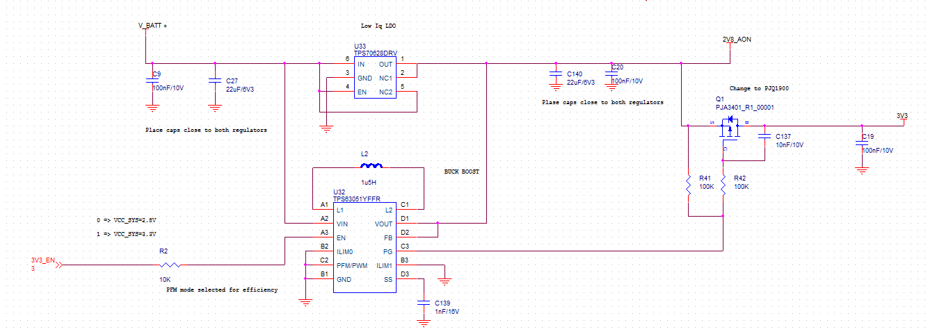
Ask a related question" button in the top right corner. The newly created question will be automatically linked to this question.

TPS63051 + TPS70628

Other Parts Discussed in Thread: TPS63051, TPS62743

I would like to power device (MCU+BLE + other) from Li-Ion secondary cell type. I need a 2.8V for powering low power MCU + BLE. Device requires a 3.3 Volts to power (for short period of time) some more demanding peripherals and for MCU+BLE too to maintain logic voltage level compatibility. My idea is to use TPS70628 linear regulator with reverse current protection, together with TPS63051 as buck-boost converter. I suspect that there will be leakage current from 2.8V to TPS63051 FB and VOUT pin. Could you say how will be magnitude of this leakage current? More generally: how big will the quiescent current in my circuit (with TPS6305 disabled)? Is there any simple, elegant and cheap solution to maintain quiescent current near 1uA?
My idea schematic picture is attached.

  • Instead of an LDO, you could reduce your power consumption even more with an ultra-low power buck, like TPS62743. You can also change the Vout between 2.8V and 3.3V on that one.

    If you still want a buck-boost to get 3.3V from a lower battery voltage, then TPS63051 is a good choice.
  • Hi, Damian

    I have measured the data in TPS63051 EVM. The test condition is : Vin (sweep from 2.5V to 5V), EN low, and apply 3.3V/2.8V onto Vout.  Measure the current into Vout.  Remove any meters or probes on Vout and set both ILIM pins to GND so that PG floats.  

    The result shows that the leakage current is below 0.1uA. So It is OK for your application.

    Note: in my data, the positive Iout means current flow from EVM to Vout power supply.

    Apply Vout=3.3V from external

    Apply Vout=2.8V from external

  • Thank you very much for your proposal, i am checking if TPS62743 can fit project assumptions. It is buck converter. It seems to not tolerate Vout>Vin. Power path switches will be needed but i don't want to increase BOM count. However, if i spot nice opportunity to stitch together TPS62743 and TPS63051, then i will consider it.
  • Thank You for your effort. Data which you provided is exactly what i am looking for!
    If you could confirm my understanding:
    On EVM board for the TPS63051: Vout||FB pins are sinking current?
  • Hi, Damian

    Actually  as I mentioned, the positive current means that EVM board is sourcing a very small current to DC Power Supply. The measuring diagram shown below:

    So, Vout and FB pins of EVM don't sink current from DC power supply.

  • Everything is clear. Thank you very much for the great support!

  • Hi, Damian

    After double check, I found out there may be some problems in Q1 control. The function of Q1 should be turn on when TPS63051 enable and turn off when TPS63051 disable. But in the circuit, when TPS63051 enable, PG is high impedance, so Q1 turn off. When TPS63051 disable, because ILIM1=0/ILIM0=0, PG is open drain which is high impedance also, then Q1 turn off.

    Have you noticed this problem? Do I have any misunderstanding in your application?

  • Thank you for vigilance. Your understanding of application is good. Yes i noticed the problem but did not updated the published schematic. I used a npn BJT for logic function: not (EN and PG).
    Could you explain me possible purpose of complication of the PG behaviour?

  • This PG behavior gives flexibility to different applications, which want a different PG behavior.