A related question is a question created from another question. When the related question is created, it will be automatically linked to the original question.
If you have a related question, please click the "Ask a related question" button in the top right corner. The newly created question will be automatically linked to this question.
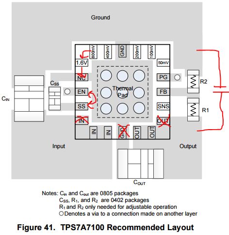
The section in the datasheet that you refer to is meant to convey layout concepts. These same concepts should be applied to the RGT package as well; however, we do not have a drawing of the RGT package at this time.
These principles can still be followed with the RGT package, much in the same way as shown in the example drawing for the RGW package.
Below I have shown the differences between the two pinouts. All of the recommendations with be the same between the two packages except for the output capacitor. The output capacitor will need to be rotated and placed similar to the input capacitor. The output capacitor will be parallel to the FB resistor network in this case and PG would still drop through a via to be routed to the desired location.