This thread has been locked.

If you have a related question, please click the "Ask a related question" button in the top right corner. The newly created question will be automatically linked to this question.

TPS7A7300 short-circuit default

Other Parts Discussed in Thread: TPS7A7300

Hello, I am currently troubleshooting a design centered around the TPS7A7300.

My reference datasheet is Rev.E (Dec 2015)
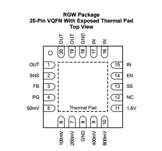
By looking at the several figures, I notice that the pin 1 marker (circle) is situated near the "IN" pins on pages 11-18. On Page 3 and in pin configuration, the marker is between the "OUT" pins (pin 1).

Is the page 3 configuration the correct one?

Also, on page 3 and on the eval module (SLAU430, dec 2012), EN is situated on pin 14 and SS on pin 13 . They are swapped on figure 43, page 25 of the device datasheet. Can I assume again that the (page 3) datasheet pin out is the correct one?


Another question:
On the Figure 43 layout example, the Css capacitor is routed through the NC pin to reach the LDO Ground via the Thermal Pad connection. On the Eval Module,  this capacitor (C4) is routed to the LDO with a via (and bottom layer ground plane))


It seems that in my design, the component has gone in short circuit (Output voltage and PowerGood are both equal to input voltage). My design is configured with a ~2.35V input and a 2.05V output (set with the user configurable pins). I have no SS capacitor and EN is pulled up via 10k to supply IN

What would be the consequence of switching the EN and SS pins? (not probable, but possible because of datasheet contradiction)

Therefore, if there is a mistake in the datasheet, EN would be left floating, and SS would be pulled up to a fraction of supply in (potentially damaging the soft start delay block, but it is within the Absolute ratings.)


I am also trying to analyze whether my component could have overheated. In standard operation, the device would be limited to 3 A and 0.3V dropout, which is roughly a 1W dissipation. [current is limited upstream]

My ground plane is extremely large (> 8 square inches), and thermo-gun analysis never showed excessive heating.

In the event of an output short circuit, the component would see 7 W, which would be painful for the component, but would activate thermal shutdown. I have never observed thermal shutdown (ie, my output was always at expected level, before I have encountered my default). Is there any possibility of having the component permanently thermally damaged before ever observing thermal shutdown?

Thanks in advance

  • Hi Ludovic,

    The Pin Configurations section on page 3 of the datasheet is correct.  Thank you for pointing out the inconsistencies.

    The pinout of the TPS7A7300 has been the same since it released.

    From what you described, I do not believe it is likely that you are running into thermal issues.  

    A schematic (just around the LDO would be fine) and a scope shot with Vin, Vout, and Iout will help me to help you debug.

    Often when the output of the LDO is at a value other than the set value, there is an unintentional leakage path which is biasing the output high.  These unintentional leakage paths can be caused by flux.  Also some loads that require multiple rails sometimes have a leakage path which can bias the lower voltage rail.  Due to topology, TPS7A7300 will not pull down the biased output.  Is there anything downstream from the TPS7A7300 that sees this 2.35 rail?

    Very Respectfully,

    Ryan

  • Hello Ryan,

    Sorry for the long delay, we have a busy end of year period.

    I have been unable to test for any unintentional leakage path caused by flux or else, the component had already been replaced due to project delay constraints. The default has systematically appeared after conformal coating (sprayed, silicone based). I have never heard of leakage paths created by conformal coating, but I would be open to any guidelines concerning any specific steps we should take in our industrial process.


    Our boards are cleaned by isopropyl alcohol, then dried 15 minutes at 85 °C. The board is then left in ambient to cool to <50°C. Then we apply our masking agents where needed (none immediately near the LDO). The board is then put 15 additional minutes at 85 °C. The board is then coated. The board is then dried 12 hours in ambient then a further 24 hours at 85 °C.

    This is done in a clean environment and coating uniformity is UV-controlled.

    The 2.35 V rail is solely used by the TPS7A7300. The LDO output is an active load following this simplified diagram.

    We have replaced the LDO and re-coated by brush. The system now seems operational, so we are indeed thinking it could be a process problem.

    Thank you for your help.

    Best Regards,

    Ludovic Bidaux

  • Hi Ludovic,

    Your diagram did not properly attach; however, I do not think I need it for this answer.  I would recommend contacting your vendor for any solder and flux that you use and ask them for their recommendations for cleaning a board.  It is possible that isopropl alcohol is not enough to remove all of the excess flux. 

    Very Respectfully,

    Ryan