This thread has been locked.

If you have a related question, please click the "Ask a related question" button in the top right corner. The newly created question will be automatically linked to this question.

LM5109A - part delays switching for a tremendous time

Other Parts Discussed in Thread: LM5109A, DCH010515S, LM5112, UCC27517A

Hello community,

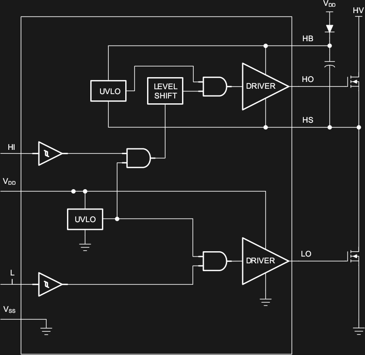
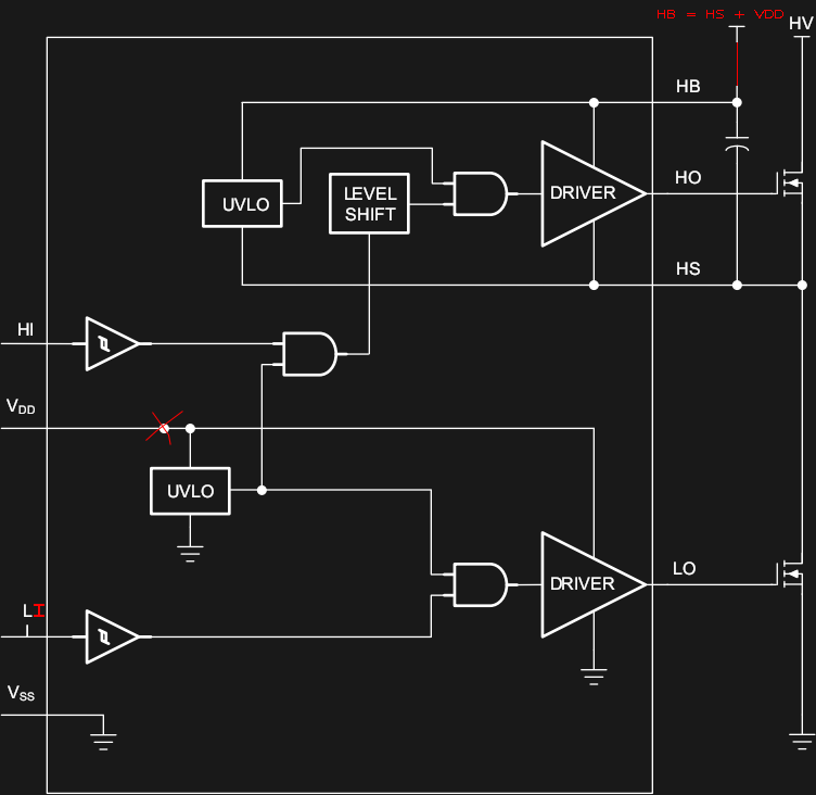
I am using the LM5109A in a step down converter. I experienced a situation where the LM5109A is not switching within tens of nanoseconds as it should but takes more than 20 milliseconds to do so.

To trigger this fault I need to unclamp all load of the converter so it gets nearly no "high"-signal at the input "HI" (maybe 1 per 3 seconds because leakage in the output capacitors of the converter (they aren't included in the wiring diagram)). Then I clamp a small load (150 ohms). This causes the fault. If I then increase the load to let's say 10 ohms then the fault goes away again. Then I can go back to a small load (150 ohms) without causing the fault.

If I unclamp all load and then clamp a big load (10 ohms) then there is no fault either.

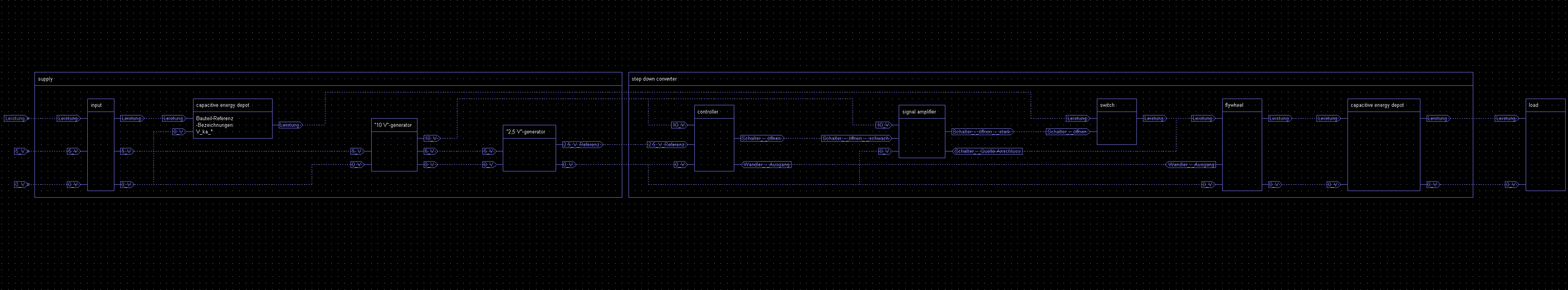
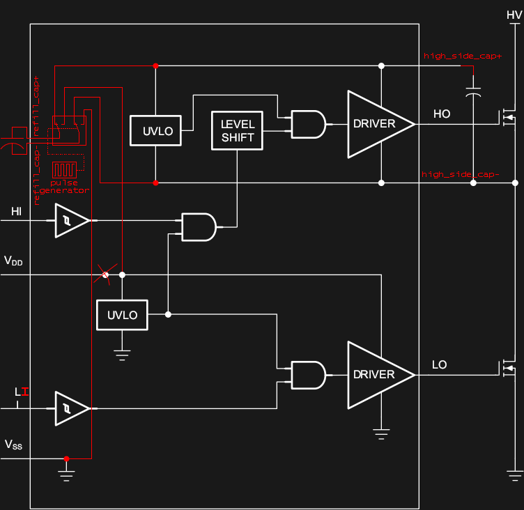
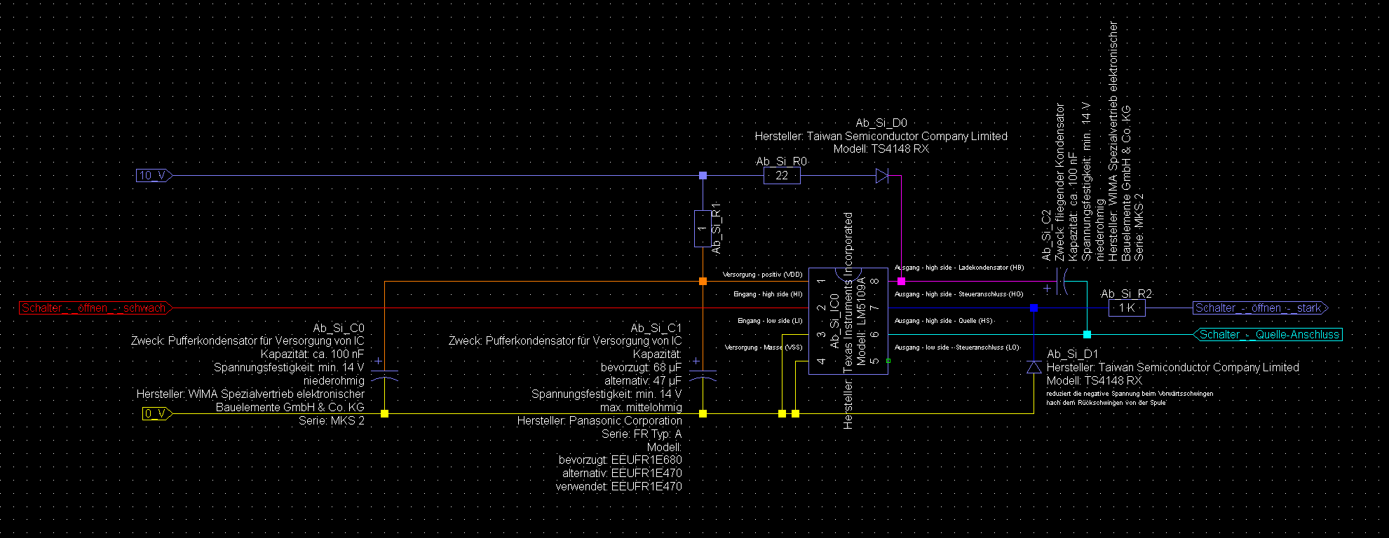
I measured all pins of the LM5109A and uploaded the diagrams together with a wiring diagram as images. I hope this helps in finding the problem and a solution.

Thank you for helping.
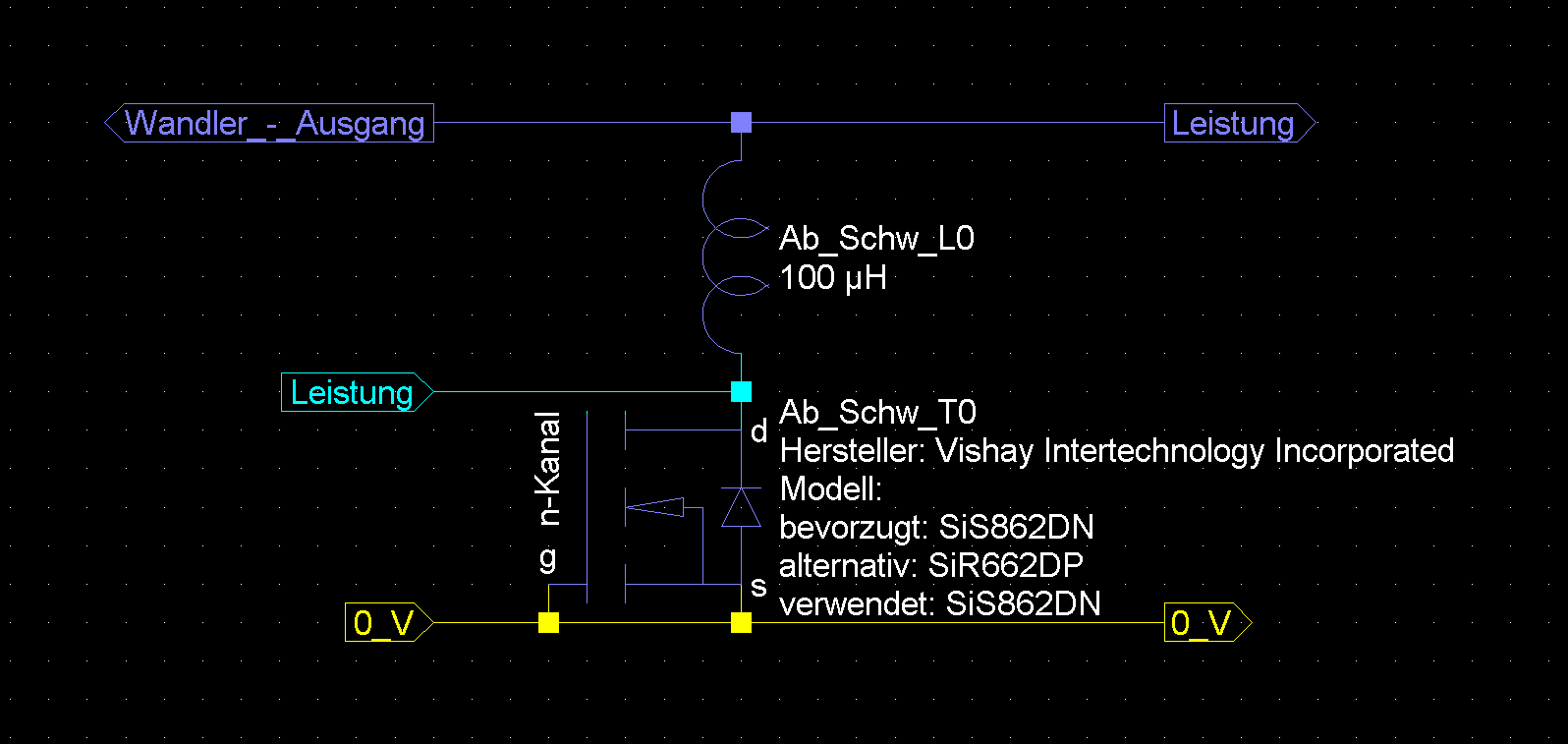
wiring diagram:

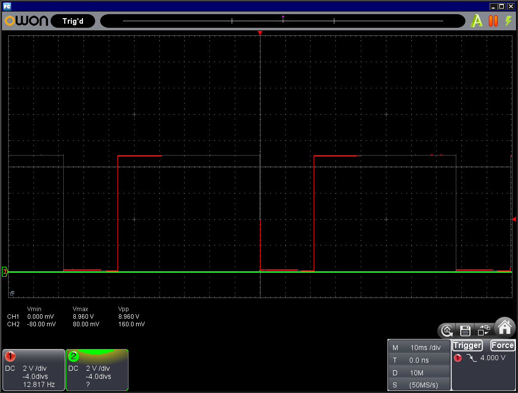
pin 1 in the fault-state:

pin 3 and 4 in the fault-state:

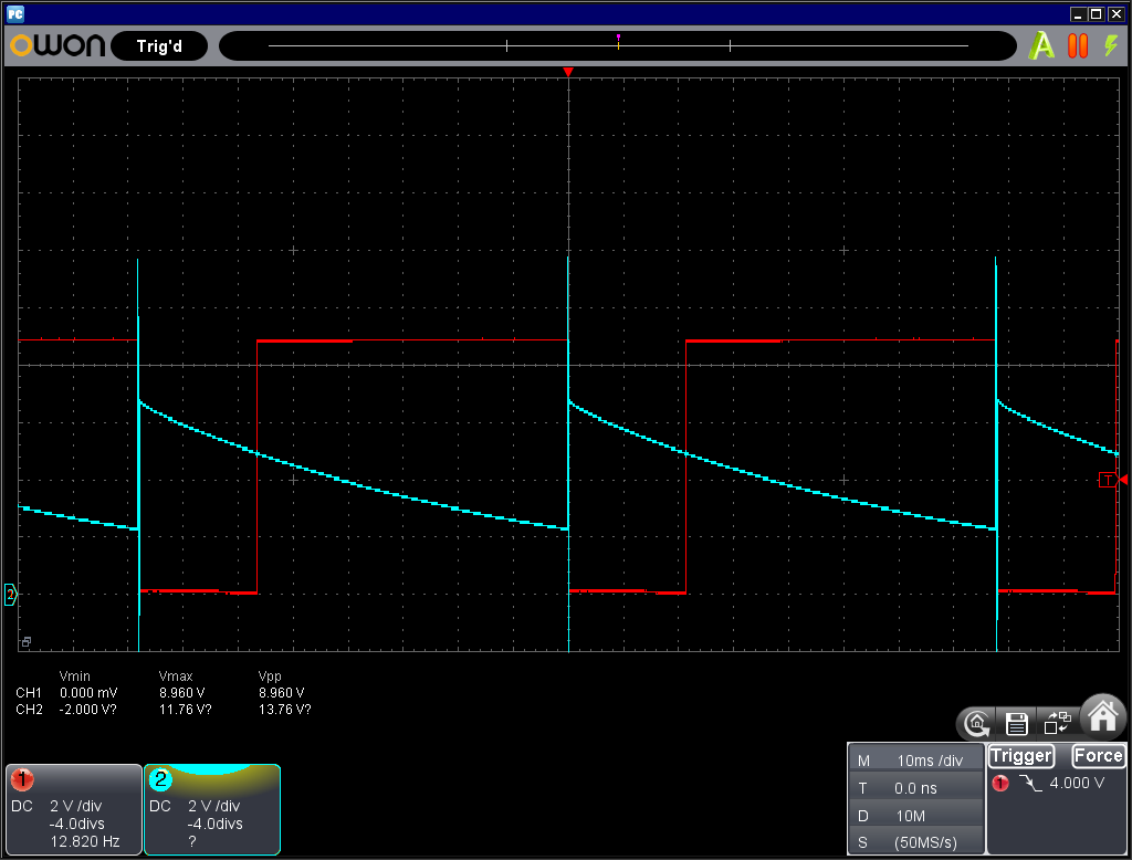
pin 5 in the fault-state:

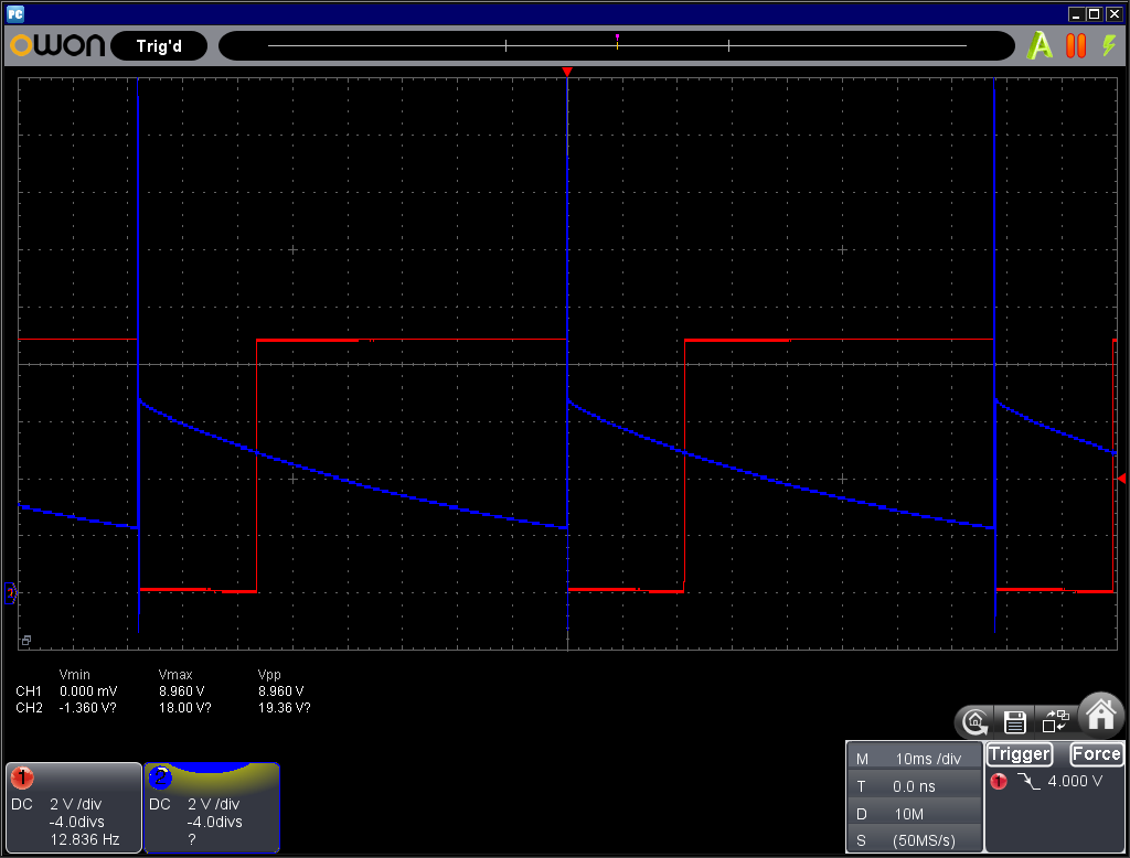
pin 6 in the fault-state:

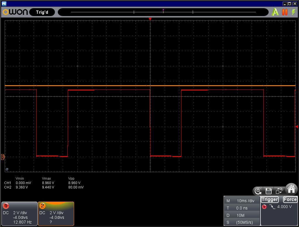
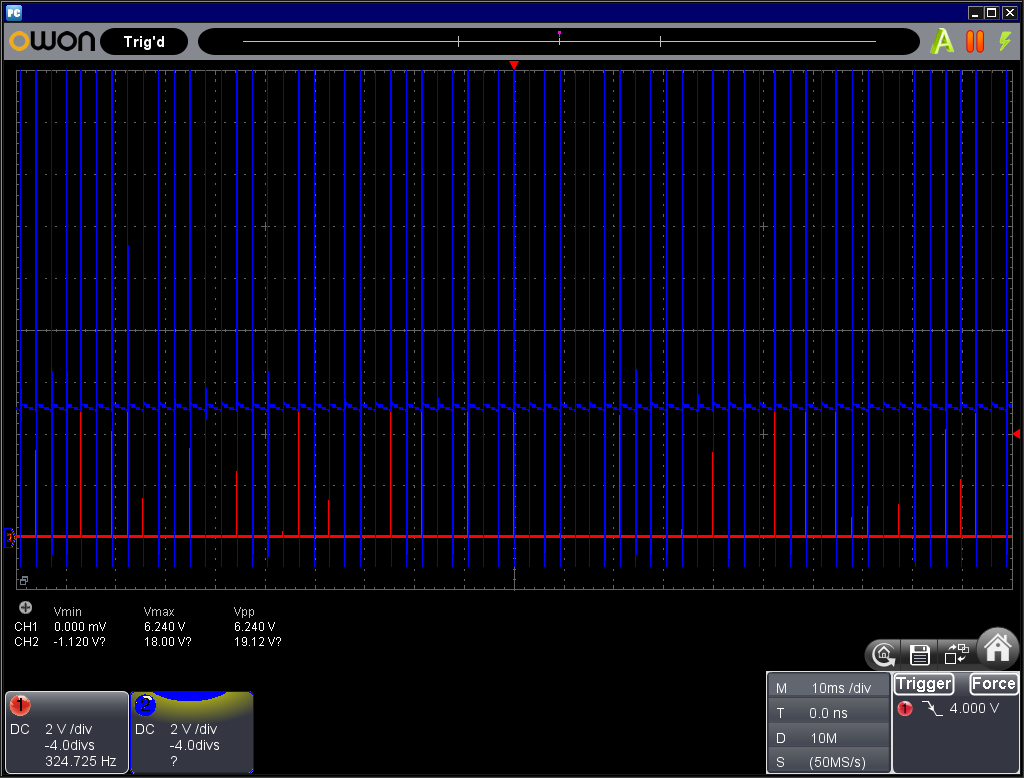
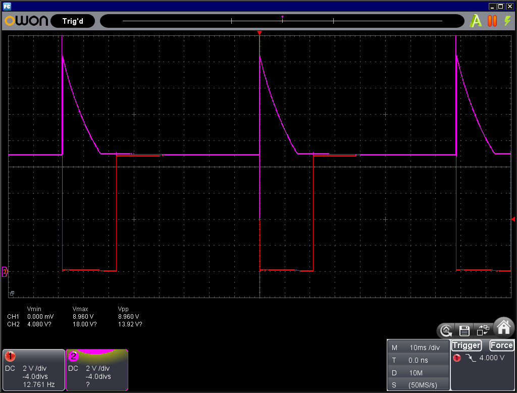
pin 7 in the fault-state - 10 ms/div:

pin 7 in the fault-state - 50 µs/div:

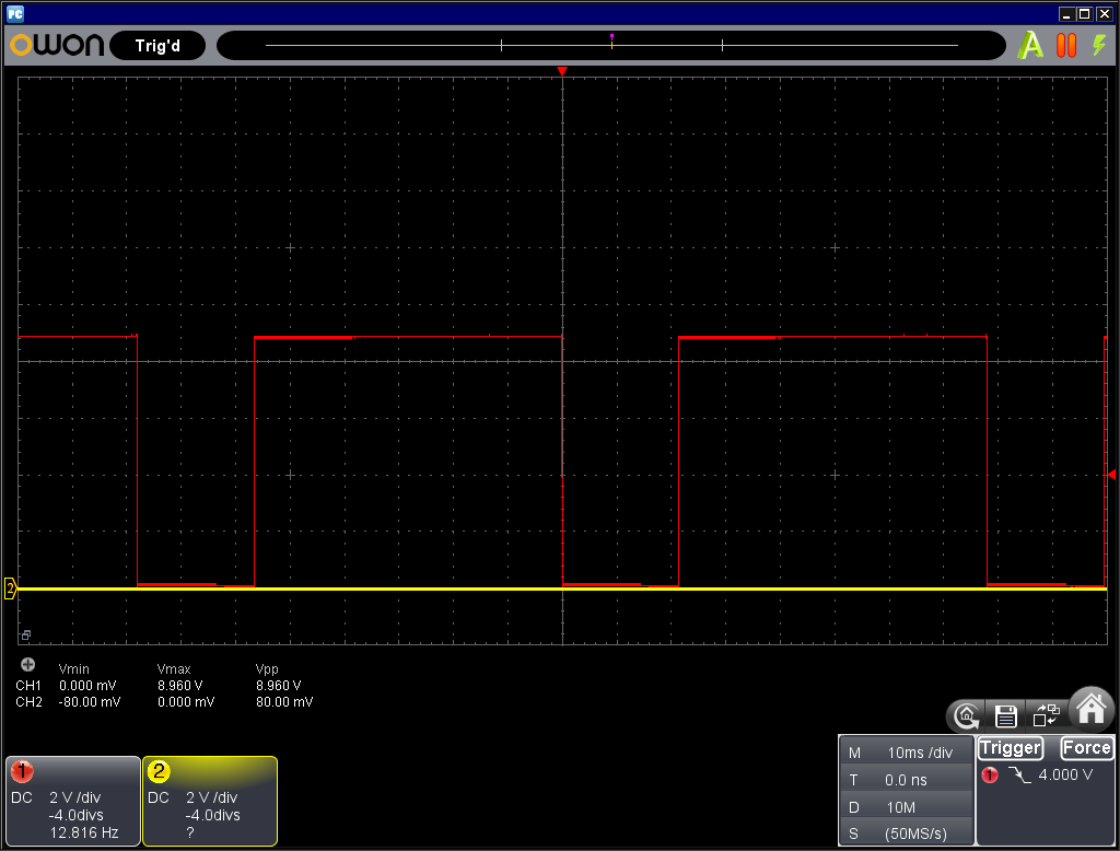
pin 7 in a non-fault-state - 10 ms/div - also 150 ohms at the output:

pin 7 in a non-fault-state - 50 µs/div:

pin 8 in the fault-state - 10 ms/div:

pin 8 in the fault-state - 50 µs/div:

I don't know whether it helps in understanding: The DC/DC converter has a bang–bang controller. This means it

- opens the switch to refill the output capacitors if the output voltage is below a certain value and

- closes the switch if the output voltage is above a certain value.

  • I will forward this to the appropriate Application Engineer to comment.
  • Firstname Lastname,

    I am the applications engineer for this device. The magnitude of delay that you mention is certainly outside of normal operation and I am here to help debug your issue. Thank you for the diagram and oscilloscope captures.

    I have a few comments/questions for which I will need your input in order to continue:

    1) Does this behavior occur if you swap out the LM5109A device for another unit? This will help understand whether the root cause is a non-compliant device.

    2) Again, thanks for your diagram. Your initial post mentions you are working on a step-down converter. Is this your actual circuit? If so, I am a unclear on how the LM5109A is being used. I see the ports to gate and source for the high-side device, but nothing connected to the LO output (pin 5). The device is designed so that the bootstrap capacitor is charged when the low-side switch is turn ON, pulling HS (pin 6) to VSS. The circuit in the diagram has no return path for the high-side source, which could explain getting undesired behavior.

    3) If the plan is to use only the high-side output, then the HS pin will need to be shorted to VSS in order to provide the return path mentioned above. Please try your tests with this condition and let me know what you see in HI and HO (pins 2 and 7). Please show plots of a rising edge and of a falling edge on HI.

    4) In your plots, "pin 7 in a non-fault-state - 50 µs/div" and "pin 7 in the fault-state - 50 µs/div," what is being shown in the red trace (CH2)?

    Please provide the feedback above so we can continue working this matter.

    Regards,

    Daniel
  • Thank you for your reply Daniel,

    1) Does this behavior occur if you swap out the LM5109A device for another unit?

    This will take me a few days. I will report back probably at the end of the week.

    2) Your initial post mentions you are working on a step-down converter. Is this your actual circuit?

    Well, it's a part of the circuit. Here is an overview:

    The wire diagram from the first post shows the block "signal amplifier".

    I see the ports to gate and source for the high-side device, but nothing connected to the LO output (pin 5).

    Yes, that's correct. It's left open. The input for the low side switch "LI" is connected to ground to prevent any action on the low side.

    The device is designed so that the bootstrap capacitor is charged when the low-side switch is turn ON, pulling HS (pin 6) to VSS. The circuit in the diagram has no return path for the high-side source, which could explain getting undesired behavior.

    If I understood the issue correctly, then the low side switch has not that much influence on whether the capacitor is beeing charged. The capacitor gets it's charge through the resistor Ab_Si_R0. The return path does not go through the low side switch but through the coil. Here let me show you a missing part of the circuit:

    The wiring diagram above shows the block "flywheel". As soon as the high side switch closes the coil starts sucking charge from wherever it can get for about 190 µs. This means that in this time the teal wire has a negative voltage. The capacitor can load for about 190 µs. But as you can see in the diagram "pin 8 in the fault-state - 50 µs/div" the capacitor only needs about 30 µs to fully recharge. After 190 µs it abruptly gets additional 7 volts. These 7 volts come from the output of the converter. The charge from the output flushes back through the coil to the teal wire.

    Please show plots of a rising edge and of a falling edge on HI.

    what is being shown in the red trace (CH2)?

    The colors match between the wire diagrams and the oscilloscope diagrams. The red diagrams in all measurements correspond to the red wire (HI). The red trace is CH1, btw.

    So far thank you for the time you have invested. I will exchange the part in a few days and report back.

  • Here is something else I found out:
    In the diagram "pin 8 in the fault-state - 10 ms/div:" you can see, that the capacitor is being discharged over a period of 15 ms. This is probably the case because the LM5109A consumes power from the capacitor. After thous 15 ms there are about 9 volts at the "+"-pin. But in the diagram "pin 6 in the fault-state" you can see at this point in time that there are about 7.5 volt at the "-"-pin. Which means that the capacitor has only a charge of 1.5 volts. This is below the lock down voltage of the high side.

    While the voltage at the output is dropping and dropping the voltage at the capacitor is rising. Finally the voltage at the capacitor is above the lock down threshold and the output of the high side is rising.

    Now I remember this situation from my first steps in using a high side transistor driver. I was aware of this conceptual problem but didn't have a working solution back then. Now I think that increasing the capacity would help leaving the fault state but wouldn't fix the problem that if there is no load for some (long) time then even a big capacitor will get empty and locks the driver until the output voltage has fallen low enough.
  • Thanks for the additional information. I will review and provide my feedback within the next day or so. As you describe, the issue may be due to discharge of the bootstrap supply. If this supply is low, you will lose the gate drive strength needed for proper performance.

    By the way, what is your switching frequency? I see from the screenshots about 80ms period (12.5Hz). Is this the target frequency? At low frequencies, the bootstrap supply does not get refreshed as often and can droop during the cycle.

    - Daniel
  • Thank you, I am looking forward to read your feedback because for me this issue is rather difficult to solve.

    By the way, what is your switching frequency? I see from the screenshots about 80ms period (12.5Hz). Is this the target frequency?

    The low frequency is due to the long unintended delay. There is also a diagram called "pin 7 in a non-fault-state - 10 ms/div - also 150 ohms at the output". This diagram shows a frequency of about 325 Hz at the same load (150 ohms). Because the converter has a bang-bang controller the frequency rises if I increase the load (to let's say 10 ohms). But currently the on threshold and the off threshold aren't set correctly. The intended frequency is probably about 400 Hz at 150 ohms. But that's just an estimation. I don't set the frequency. I set the thresholds to define the output ripple. The thresholds lead to a certain frequency but as mentioned the frequency also depends on the load.

    At low frequencies, the bootstrap supply does not get refreshed as often and can droop during the cycle.

    Yes, the discharging during the off-part of the cycle is the problem we are currently facing. The situation where the frequency is really low (1 per 3 seconds or so) when there is no load at all is the problem which I can't solve with a bigger capacitor (because it would have to be extraordinary big) or a higher frequency (because this means that the converter would output additional charge/increase and increase it's output voltage.

    The discharging during the on-part of the cycle is not an issue for me because I am currently using a 100 µH coil. If I would open the switch too long then the current would rise to insane levels and the output voltage would become too high so the bang-bang controller closes the switch before that happens.

  • Maybe this helps in getting a small step closer to a solution: I think that what's necessary is something that provides reliable power at the "HB"-pin. Something like HS + VDD.

    original:

    modified:

  • I would like to suggest something like the following circuit to the Texas Instruments team to consider implementing to fix the conceptual problem:

    Maybe you will find a better solution which causes less costs (less additional pins or no additional external capacitor).

    Till then I will try to build something like this around the LM5109A. Does someone know if an IC already exists to fulfil the task?

  • I have gone over all your posts with the additional information. My understanding is that the circuit is configured to drive a high-side switch using the LM5109A. There is no low-side switch in the application.

    The LM5109A is a half-bridge driver intended to drive the high- and low-side switches of a half-bridge using a bootstrap capacitor supply for the high-side switch gate-drive sourcing power. When the low-side device turns ON, the HS node is connected to VSS/0V, which allows the bootstrap diode to become forward-biased and charge the bootstrap diode. Without a low-side switch, the device will not function as intended.

    In your last post, you present the concept of a driver IC with an integrated charge pump to derive the high-side drive supply. At the moment we do not have such a device in our catalog.

    One way to generate the high-side supply is to use an isolated DC/DC converter such as DCH010515S. The isolated output could be connected across the LM5109A HB and HS pins. However, if using an isolated module like this, the driver could be replaced with a single-output driver such as LM5112 or UCC27517A.

    I am aware that this is a change from the existing circuit, but the design requirements for the LM5109A are not compatible with driving a single high-side switch without a path to refresh the bootstrap capacitor.

    Regards,

    - Daniel
  • Thank you for your response, Daniel.

    My understanding is that the circuit is configured to drive a high-side switch using the LM5109A. There is no low-side switch in the application. ... Without a low-side switch, the device will not function as intended.

    At the current state it's correct that there is no working low-side switch. I left out the low-side switch control circuit to avoid additional complexity before I have fixed the recharge problem. As you can see in the circuit with the coil there actually is a low side switch but it's gate is always connected to ground. My plan is to add the control circuit to drive the low-side gate later. But currently I only use the body diode of the transistor.

    From my understanding opening the low side switch would not solve the problem at all. It wouldn't even improve the situation. Actually it would even make it worse. That's because I would only be able to open the low-side switch during the time when there are below 0 volts at HS pin/negative connection of the capacitor. As soon as the energy in the coil is depleted I need to close the low side switch again. Otherwise the output capacitors would discharge through the coil and then through the low-side switch to ground. In other words: By having a working low-side switch the bootstrap capacitor would get no additional time to charge. Currently the capacitor is charging in the exact time when I could open the low side switch at best. Opening the switch would increase the voltage at the HS pin to slightly below 0 volts because the voltage drop over the transistor would be lower than the voltage drop over the body diode is. Currently it's quite somewhat below 0 volts (-1.6 volts or so). The absolute voltage at the capacitor during the charging time would be lower if I'd open the switch. Lower voltage on the capacitor means that it's going to be even faster depleted. That's why I said that opening the switch would even make the situation worse.

    I hope this helps in understanding the conceptual problem with the part which exists independent of the fact whether you have low-side switch. Other parts which work in a similar way are probably also affected.

    One way to generate the high-side supply is to use an isolated DC/DC converter such as DCH010515S. The isolated output could be connected across the LM5109A HB and HS pins. However, if using an isolated module like this, the driver could be replaced with a single-output driver such as LM5112 or UCC27517A.

    Yes, using a low-side driver in this situation is halfway possible, too. You'd still have to use a level shifter to get the control signal to the input but low-side drivers usually have better values than high-side drivers have. Parts like the DCH010515S have a current consumption of more than 60 mA when outputting 1 to 3 mA for the LM5109A. :-/

    I appreciate your efforts. But currently it looks as a charge pump solution is more practical.