hello
Here are some questions about pl455's balance function want to consult you
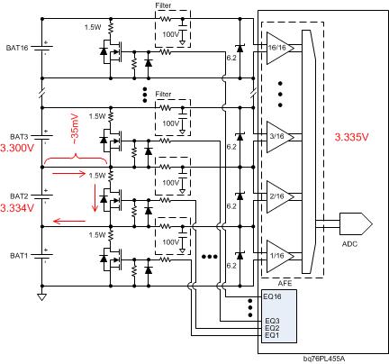
1、the cell's voltage will be changed when i turn on the balanced switch and there was a beat voltage with 5mV ~ 20mV on the next battary?
for example
the cell n's normal volt is 3450mv ,the cell n's volt will be up to about 3456 ~3460mv when i turn on EQ(n-1)
why so?
2、It's about the "TSCONFIG" reg address is 0x1E, the BIT5 (EQ_SQUEEZE_EN) can not be written 1 ,I want to test the open wire detection funciton
and so how can I write the 1 to it ?
3、The power of VIOREG ,can be use to the VIO in single mode?