This thread has been locked.

If you have a related question, please click the "Ask a related question" button in the top right corner. The newly created question will be automatically linked to this question.

Help on the UCC29950 for frquency related

Other Parts Discussed in Thread: UCC29950, TL431, UCC27750

Dear Friends,

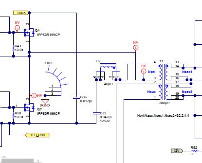
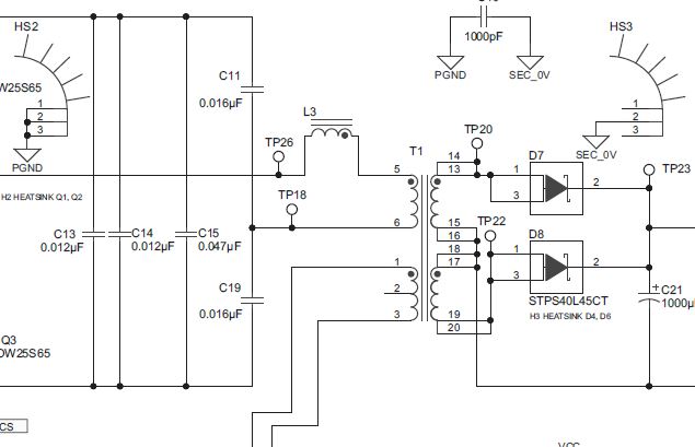
We are developing project on the UCC29950

We are taking a reference from the ucc29950evm-631

At first, i want to ask you that what is the Frequency of converter..? 

How to design the transformer/inducto for the Same..??

Is it fixed frequency or variable..??

Kindly help me for the same.

Thanks

Deepak C

  • Hi Deepak,

    The PFC stage is fixed frequency and from the datasheet (o UEVM User Guide) it various from 87 kHz to 109 kHz including dithering. The LLC can vary from 63.7 kHz MIN to 378 kHz MAX also from the datasheet.

    I assume you are interested in the LLC transformer which is a Renco Electronics part number RLT1-115. Do you happen to have a contact with Renco Electronics since I see they are not providing the transformer specification in my quick search on the Internet.
  • Hi Brian

    Thanks for reply.

    i understand that the frequency is variable and it is function of fb pin voltage.

    For EVM Schematics, what frequency have you considered..?

    so that, we can design the transformer at that frequency.

    I had an contact with the Renco for transformers, it seems a 40 $ costing for the single transformers.

    i want a detailing of Basics LLC Converter whether it is operating on the fixed frequency or Variable.

    Hope yours doubt clears

    Cheers

    Deepak C

  • Hi Deepak,

    We use our UCC29950 design calculator found in the tools tab for this PN: www.ti.com/.../toolssoftware

    I believe the nominal switching frequency is set for 120 kHz even though the LLC is a variable frequency control.
  • Hi Brian

    Thanks for the software provided.

    i read the Excel sheet where they have mentioned of frequency 120khz

    But When i was checking the EVM module of 12 volt/25AMP where the fb pin voltage is above 3 volt

    and if you look the graph of FB Pin vs Switching Frequency then it is misleading (How 120 khz will we get..??)

    Thanks

    Deepak C

  •  Which schematic to refer.??

  • Check above 2 circuits.. where almost capacitors position are different.. and what the Cr in the circuit both circuit..??
  • Hello Deepak

    Cr is C39 in the first circuit, Cr is the parallel combination of C19 and C11 in the second circuit. Either circuit will work and further information is in section 8.2.2.16 of the UCC29950 data sheet.

    The LLC stage of the UCC29950 acts as a voltage to frequency converter, the voltage at the FB pin programs a certain frequency at the GDx pins according to the graph in Figure 1 of the data sheet. 120kHz corresponds to about 1.7V at the FB pin.

    If the FB pin is between 3V (approx) and 3.6V the frequency will be a fixed 350kHz. If the FB pin gets higher than 3.6V then switching will stop. If switching stops the Vo will drop and FB will then drop too. When FB falls to 3V switching will start again. This burst mode will continue until the load increases.

    Regards
    Colin
  • FB pin programs a certain frequency at the GDx pins..??

    What is GDx..??

    if you look at the schematic..

    Aplly KVL,

    +VCC-Vce(on)-I(1.2K+3.32K)=0

    So,Current flowing through the Loop will be i=2.6mA

    So,voltage drop across 3.32 (FB Pin)=2.6mA*3.32K=8.7V

    What calculations are you doing or giving..??

  • Hello Deepak,

    I am interested in learning about your application and who you work for, can you send me your answers to my email account b-johnson@ti.com?

    Designing the LLC transformer requires an estimate of the max load Fo and min load Fp operating frequencies since the regulation on the LLC is going to be between these frequencies. The 120 kHz is the target design nominal full-load switching frequency Fo. But for regulation we use a wider range of switching frequencies which is the point to using Figure 30 in the datasheet. This is how you go about designing the transformer.

    Fb versus switching frequency takes into account the other losses not estimated in the deign of the transformer and measurements include non-ideal effects like offsets, etc.

    How did you model the opto's in your KVL equation? The opto's are controlled current sources.
  • Hi Brian,

    I am considering it as Transistor model, cant we apply a KVL there..?? i dont know exactly..??

    it is related with the CTR something..??

    What equation will be at transistor side..?

    can i use pc817 insted ACPL-217-56AE..??

  • Hello Deepak

    GDx is a short form for the signals GD1 and GD2.

    So,voltage drop across 3.32 (FB Pin)=2.6mA*3.32K=8.7V - this is the maximum voltage at the FB pin with these resistor values and assumes that the phototransistor is saturated. As you know, the FB pin control range is VFB(min) (170mV) to VFB(max) (3.88V) so we can comfortably exceed VFB(max) with these resistors. The current in the phototransistor when the FB pin is at VFB(min) is 51uA (170mV in a 3.32k resistor). This is reasonable - but you should double check the phototransistor leakage current at high temperature when the LED current is at zero and maybe reduce the 3.32k value if necessary. The important thing here is that the emitter of the phototransistor has enough operating range to set the FB pin at any voltage in the range between VFB(min) and VFB(max). So the phototransistor current has to cover the range 2.6mA to 50uA. The phototransistor current is simply the LED current multiplied by the CTR and it is easy then to calculate the LED currents needed to give the phototransistor currents. A slight complication is that the CTR is a function of the LED forward current and of temperature - so you need to calculate the required LED currents with this in mind and also with the part to part CTR variations that you will get. It is also true that the CTR of all optocouplers degrades with time - I've never been able to get a quantitative description of this degradation but the rule of thumb is to assume that it can halve over the product lifetime. You will also need to do the calculations with this factored in.

    So, you should be able to calculate minimum and maximum values of LED current. This allows you to select the operating current for the TL431. Note that it is usual to include a resistor in parallel with the LED. This provides a path for the minimum Ik of the TL431. The resistor should pass the minimum Ik with a voltage drop less than the Vf of the LED - for example we have used a 10k resistor to pass 100uA at 1V. You may want to use a lower value resistor - it depends on the minimum Ik of the TL431 you are using.

    Now, can you use PC817 instead of the ACPL device ?. There are two considerations here. First, from a technical point of view there is no problem using a different optocoupler, you just need to do the calculations based on the device parameters given in the data sheet. Second - and more importantly - the optocoupler crosses the safety isolation barrier and you must make sure that any part you choose to use (including the ACPL device) meets the safety isolation standards that you require. TI can't offer you any advice on this safety related issue and I'd suggest that you get advice from your safety approvals experts before making a final selection.

    Regards
    Colin
  • Thanks colin.. Well understable explanation..!!
    Are there any help for the Transformer and inductor design..??

    Can i take a random core with the Known AL Value.. wound turns to achive the 50uH Inductance ..?? will it is good idea to move ahead..?

    Deepak C
  • Hi Deepak,

    The optocoupler is a current controlled device, look at figure 3 in the following link: powerelectronics.com/.../Kollman and Betten September 2003.pdf
  • Thank you Brian..!!

    Help me on the Magnetics..

  • Hi Deepak

    The best starting place is to look at the magnetics design cookbook which is at www.ti.com/.../slup132.pdf written by Lloyd Dixon. This paper is one of the TI power seminar white papers and the fill collection is at www.ti.com/.../login.shtml . The material in the 'Basic Magnetic Technology' and 'Magnetic Component Design' is also relevant.

    Unfortunately magnetic design isn't straightforward - at least if you want to get the best performance out of the magnetic. You should be able to get started with the information in the references above. Do feel free to post any further queries you may have.

    Regards
    Coliln
  • Hi Deepak,

    I also suggest you contact a magnetics vendor, I will send you a contact in your private email.
  • Hi Brian,

    We successfully tested the PFC_GD Signal and able to get the 98khz /90% duty cycle signal..!!


    Now we are facing problem for the GDX Pins.

    I am unable to get the Waveforms on the GDx pins..

    I am feeding a external Voltage at fb(with the help of External supply) of (0.2-3V), but ic does not taking any actions.

    Few of Observations here,

    a) When i am exceeding a FB Pin voltage 1.3 voltage then the PFC_GD signal get dissappered. (Dont know why..??)

    b) PFC overvoltage is working properly (If i exceeds the voltage on the Vbulk pin above 1.0 V then pfc_gd signal should dissaper and it is happening)

    My doubts..
    1) Is llc_cs signal is necessary to provide..?? if yes then how i can provide externally.(Voltage should not exceed the 0.7v as per the datasheet)
    2) We are using the Aux mode here.
    3) Do i need to make the Feedback circuits and and provide the same to the Circuit (For FB Signal)-> We have to check the FB Pin Voltage Vs LLC Frequency.


    Kindly Help
    Also i will be available on deepak.chikane@gmail.com

    Regards
    Deepak C
  • Hello Deepak

    Good that you can get the PFC stage running -

    Getting the LLC running should be relatively simple but do remember that the LLC will run only if the PFC is running.

    The LLC_CS signal is used only for over current protection - the LLC will run even if it is tied to ground.

    The MD_SEL/PS_ON pin must be close to VCC to enable LLC operation - if you are using VCC = 12V then the MD_SEL/PS_ON pin must be greater than 10.9 VV [VCCAB_UVLO(start) ]

    The VBULK pin must be above 0.77V (VBULK(llc_start)

    The feedback pin must be in the range 0.2 < VFB < 3.6

    The PFC stage should be running too

    Do let me know how you get on.

    Regards
    Coliln
  • But why the PFC waveform is vanished if FB pin voltage varied externally above 1.5V.

    I will do the same as provided for LLC procedures..

    I am from india so our work time is 9-6 pm are any application engineers available in this time in forum so I can quickly do the same and reply now I am at home..will do same changes tomarow and if update you.

    Thanks for the help.
  • Hello Deepak


    That's a good question and I don't know the answer. The PFC should continue to operate providing that the input line voltage is still present and the MD_SEL/PS_ON signal is greater than 25% of VCC (VPS_ONPFC_RUN).

    If the LLC is not running then the PFC stage is unloaded and it will go into a burst mode and the intervals between bursts can be quite long.

    The PFC stage is not affected by the voltage at the FB pin - they are completely independent. That is why I'd suggest that you get the LLC stage running correctly and then we can look at why the PFC stage stops. Can you send your schematic to me at colingillmor@ti.com  and I'll have a look at it.

    Regards

    Colin

  • Allready Failed 2 ics during  start up.

    By keeping my power supply in cc mode..

    now, how the pfc can make it loaded..??

    Do i apply some capacitance or something..??

    or pfc driver..???

    What is burst mode..??

  • Hello Deepak

    The AC source cannot be operated in CC mode - by it's nature the current from this source varies sinusoidally.

    You should have some capacitance at the PFC output - something between 0.5uF/W and 2.4uF/W. The UCC29950 is fully internally stabilised and does not need any external compensation network for the PFC stage.

    Thanks for the schematic - I'll reply to your email account shortly with comments on it.

    Regards
    Colin
  • Hi Colin,
    I am doing the basic testing so i am not connecting Any mosfets and inductor or bulk capacitors now.
    I am having a pfc+llc control board on one side and i made one main board.

    Before connecting it to the Main Board,
    i will test whether the Pfc_gd and GDx Signals are fine.

    for the Basic functional testing,
    My points are
    1) PFC_CS-> Tied to GND
    2) LLC_CS-> Tied to gnd
    3) VBulk-> 1 Volt (External power supply)
    4) SUFS->+VCC
    6) SUFG->LEF OPEN
    7) FB-> 0.2<FB>3.6V (External power supply)
    8) AC1 and AC2 Diretly from the variac and resistor divider
    9)AGND and GND Shorted
    10) AC_DET-> left Opened
    11) MD_SEL/PS_ON-> By switches (pfc one switch and llc one switch)
    12) PFC_GD-> Not connected anywhere (R30 Removed)
    13) GD1-> Not connected anywhere (R25 Removed)
    14) GD2-> NOT Connected anywhere (R24 Removed)


    Now let me know where i am failing..??

    Regards
    Deepak
  • Making the same connections..

    Now, in my circuit

    I am continuously getting the AC_DET SIGNAL=High

    Instead of applying the AC Voltage, i am not able to get the PFC Waveforms.

    I have followed the sequence of turn on

    1) Apply +VCC

    2) WAIT FOR 1 Second

    3) Apply MD_SEL/PS_ON=5V (by switches)

    4) Apply Vbulk=0.8v

    5) Aplly ac voltage..

    Observations:

    1) No PFC Waveform

    2) AC_DET=High=4.7V

    Any ways to troubleshoot, pls help

  • Hello Deepak

    AC_DET goes high if the controller does not detect the zero crossings of the AC waveform - so I'd suspect that the signal at AC1 and AC2 is not correct for some reason.  Here is an image of what you should be seeing at the AC1 and AC2 pins. The Line voltage was probed with a differential probe. The other waveforms are relative to the GND pin. The initial 'spike' on AC1 is due to some internal configuration of the the UCC29950 and is normal - it may also appear on AC2, it jjust depends on timing. What you should see is the waveforms arrowed. The amplitude will be function of the line voltage. The UCC29950 will act on the current levels into these pins - according to the levels given in the datasheet - I'd suttest you start with a line voltage amplitude of 115V or so.

    If you don't see the waveforms arrowed (and they MUST be 180deg out of phase too) then we will need to look at how you are generating them.

    Let me know how you get on - also, do let me know if the image below transferred successfully - I can see it as I type but I don't trust this s/w to deliver it correctly   (!)

    Regards
    Colin

  • Hi Colin

    I got the Waveforms (Both PFC and LLC)

    There is an Voltage at VDD pin should be above +14V

    I was testing the same as a week on +12V Supply and it was giving me a Only PFC Waveform.

    For system and final testing

    now, i am bypassing the PFC and

    LLC will turn on at the 300VDC Generating by the Bridges to avoid the BVDSS.

    I am having mosfet of +500V with 10amp 

    Will update the same tomorrow.

    Regards

    Deepak C

  • Hi Colin,

    Happy New Year.

    as i have started the LLC Only, bypassing the PFC Sections.

    My observations are
    Input dc voltage:350VDC
    Output voltage at no load:16VDC

    Output voltage with 3 amp =12.4V

    As i am expecting the output of +12V at the current of 20-25AMP

    But at the regulation, i am having problem for the regulations 16V to 12V with 3 amp only.

    Are there any changes needs to be done.
    i have allready changed the Optocoupler to PC817 instead of PC3H7J

    Are there any troubleshooting points.

    Do you have time for skype so we can discuss further as project timeline allready exceeded
  • Hello Deepak

                    Unfortunately I have a hard deadline for a conference presentation today so I won’t be able to skype you. In any case TI won’t use skype – but we do have conference call alternatives.


    The first thing I would check is that the UCC29950 controller is ‘doing what it is told to do’.

                    Check the voltage at the FB pin and the switching frequency of the LLC stage (GD1 or GD2)

                    Is the FB voltage lower than expected. See my comment in red below.


    Then check your FB amplifier chain.

                    Turn the LLC power train off – dc input voltage = 0V


    Apply a variable back bias voltage to the system output – a small 0 to 20V supply would do this nicely

    Start at 0V and increase slowly. Monitor the output of the error amplifier (TL431 cathode) and observe that it goes low as the back bias voltage is increased past the expected regulation point.


    Check that the voltage at the FB pin also goes from low to high as the back bias voltage increases past the regulation point – you will have to apply VCC to the UCC29950 and the optocoupler collector to do this.


    If the FB pin is being adjusted up and down as the back bias is moved above and below the regulation point then you can be fairly sure that the feedback signal is ok. FB should be low when Vout < Vreg and high when Vout > Vreg


    Let me know how you get on – I’ll keep an eye out for an email from you.


    Regards
    Colin


    From: Deepak Chikne [mailto:deepak.chikane@gmail.com]
    Sent: 06 January 2017 10:43
    To: Gillmor, Colin
    Subject: Re: Help on UCC27750


    Hi Colin,


    Happy New Year.


    as i have started the LLC Only, bypassing the PFC Sections.


    My observations are 

    Input dc voltage:350VDC

    Output voltage at no load:16VDC          What is the LLC switching frequency?, Is the LLC running continuously or is it in a burst mode? Does Vout adjust up and down as Vin is adjusted up and down (ie no regulation) cg