Greetings!
I have designed and prototyped the following 5V to 13V boost regulator (max 600mA) using the LM3478 and need a bit of help troubleshooting a noise problem. Here's the schematic (all caps are SMT ceramic unless otherwise noted):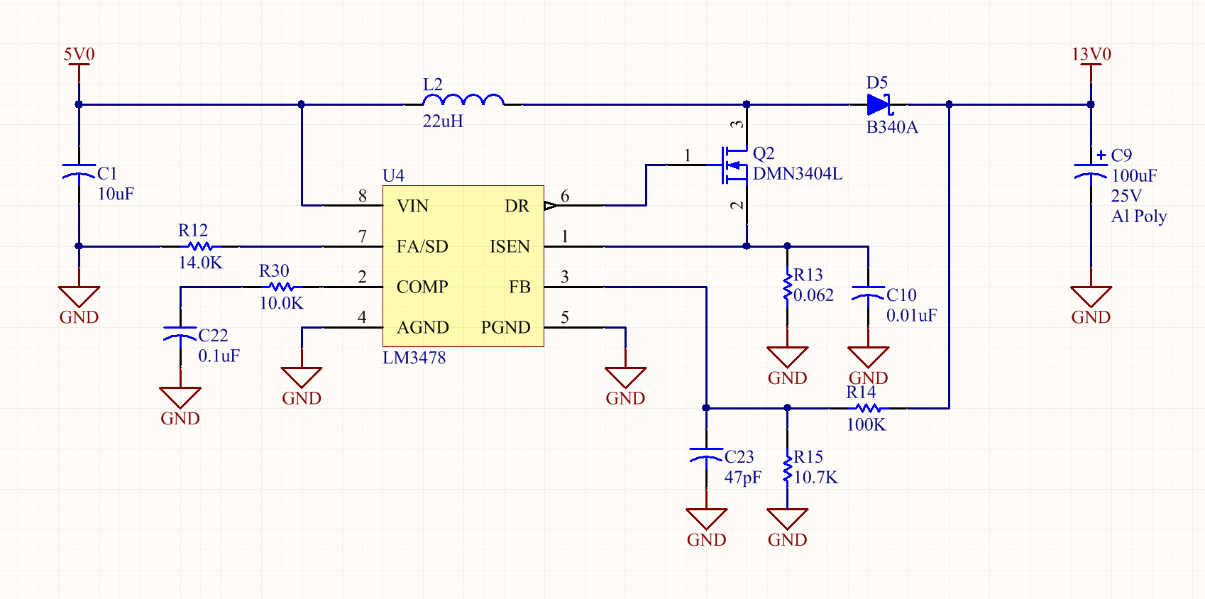
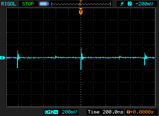
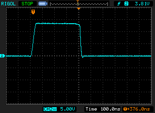
The circuit pretty much works, except that I see noise spikes of around 300mV pk-pk on the output under a relatively light 10mA load measured directly across C9 using an oscilloscope probe with a short ground:
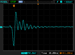
Here's a close-up of one of those pulses:
It seems to me that these noise spikes are way too big and that we will fail EMI, but I have not been able to eliminate them. Can you please help?
An astute observer will note that the period of these noise spikes is equal to the period of the LM3478 switching frequency, about 800kHz. The largest spikes occur (shown above) when the MOSFET switches on and the voltage on the switching node drops to zero.
Speaking of the switching node (on the drain of Q2), the waveform looks pretty decent. I don't see the large underdamped oscillation that would indicate the presence of significant stray L and C in the PCB design. There is, however, a bit of undershoot prior to the rising edge and negative overshoot after the falling edge.
I also measured voltage at the Source of the MOSFET, directly across the current sense resistor R13 and saw the following noise. I expect this node to be fairly noisy, but these noise spikes coincide very closely with the ringing on the output voltage. Correlation or causation?
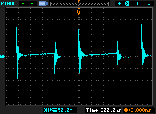
I have tried capacitors of various values across R13. Each one changes the characteristics of the ringing in image above (mostly different natural resonant frequencies) but doesn't significantly reduce or eliminate it. I also observed that the ringing seems to get worse when I use a shorter ground lead! When I use the usual 3 inch ground lead on the scope probe, the ringing appears to be much lower amplitude than when I use the short piece of copper wire looped around the ground tab of the scope probe. This is the opposite of what I expected! In my experience, the stray inductance in a long ground lead tends to form a resonant tank circuit with stray capacitance on the PCB leading to phantom noise on the scope that isn't really there, but that's the opposite of what's happening here!
In conclusion, I have the following questions:
- Are the 300mV noise spikes really something to worry about or should I expect them in a Boost regulator design? Because the noise is only 2% of the output voltage, the system will work fine. I'm worried about EMI.
- What is the root cause of the output noise? Is it caused by the diode junction capacitance interacting with stray PCB inductance? Could it be purely an artifact of PCB stray L and C? Somethign else?
- Can I add a snubber somewhere to get rid of the noise? In parallel with the diode, perhaps?
Any help is much appreciated.
Cheers,
Scott