


Hello,
Question 1: How can I calculate the modulator gain for TPS40054?
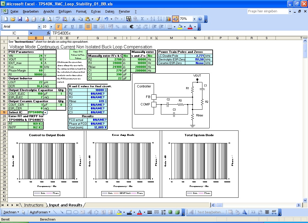
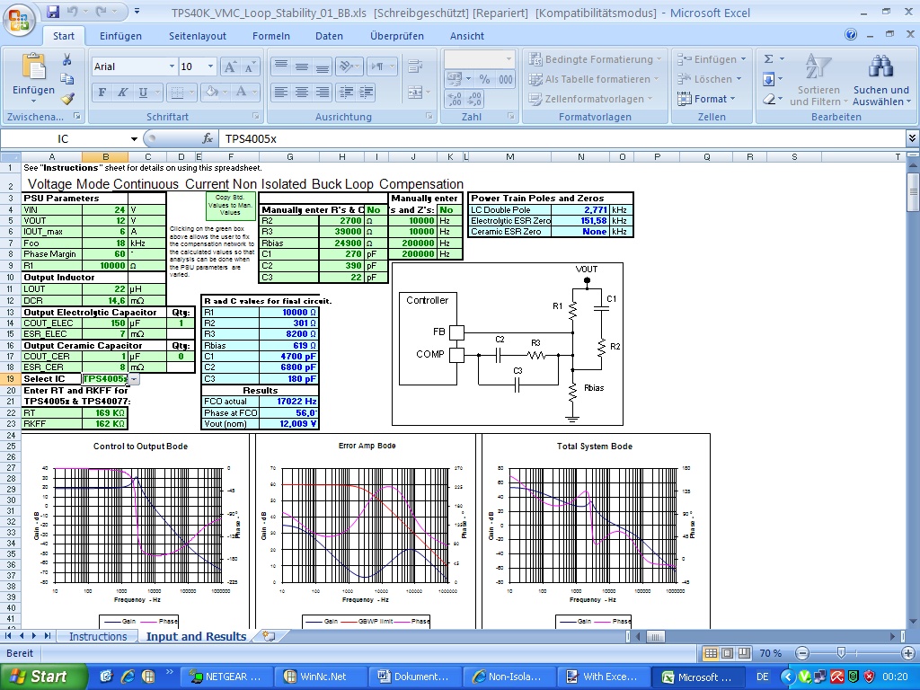
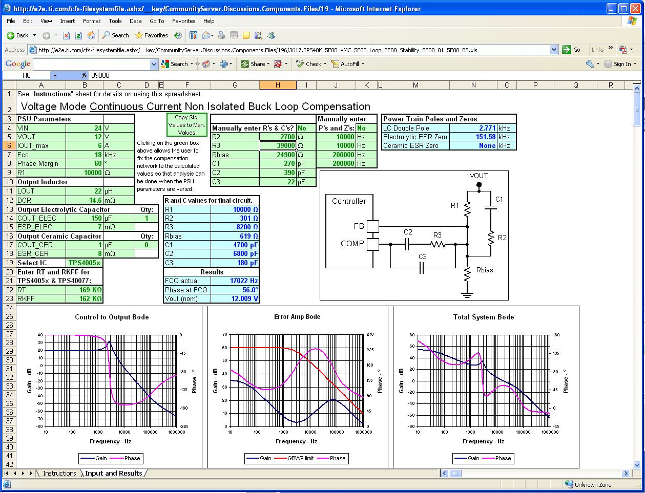
Here are the specifications:
Vin_min=18V, Vin_max=30V, Vout=12V, Iout=6A
I have found the following equations by TI: (http://focus.ti.com/lit/an/slva301/slva301.pdf)
Amod = Vcc / Vramp
Where the Vramp = 2 x (Vcc - 3.48) / (Vuvlo – 3.48)
1) Which value can I use for Vcc? Vin_min or Vin_max
2) Which value can I use for Vuvlo?
Question 2: Value of Resistor Divider
Which value can I use for R1? Data sheet of TPS40054 page 17: tell me 50K to 100K but SwitcherPro use 10K?
Thank you.

