Hello,
I am getting failure after using the enable pin on this device. The failure seems to be a short issue that develops after triggering the enable pin. I have attached my schematic and have uploaded a couple videos to demonstrate the issue.
Based on what I have provided, is there something I should change to correct the problem?
Videos:
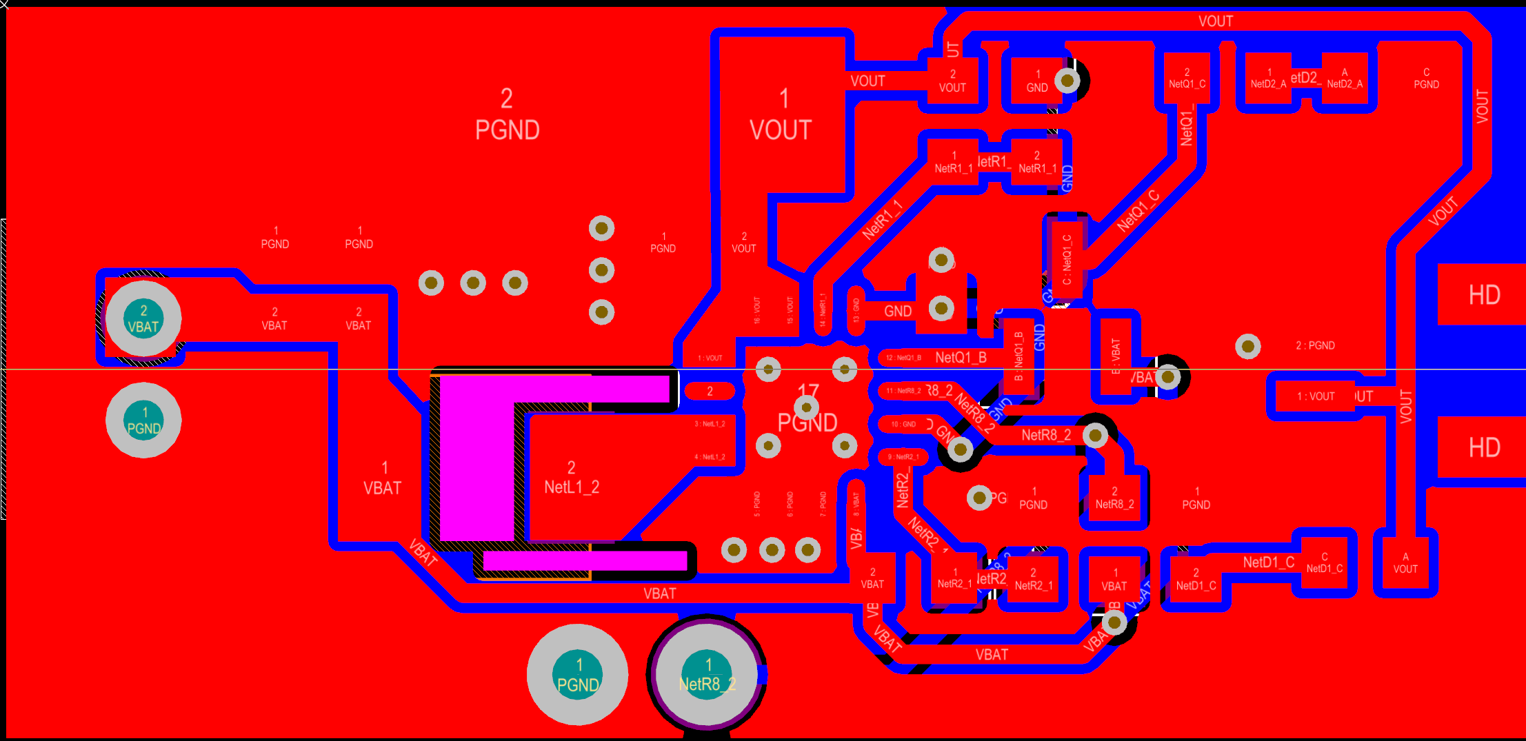
Schematic: