This thread has been locked.

If you have a related question, please click the "Ask a related question" button in the top right corner. The newly created question will be automatically linked to this question.

TPS2492: TPS2492 switches off when load is applied

Part Number: TPS2492
Other Parts Discussed in Thread: CSD19536KTT, CSD

Hi,

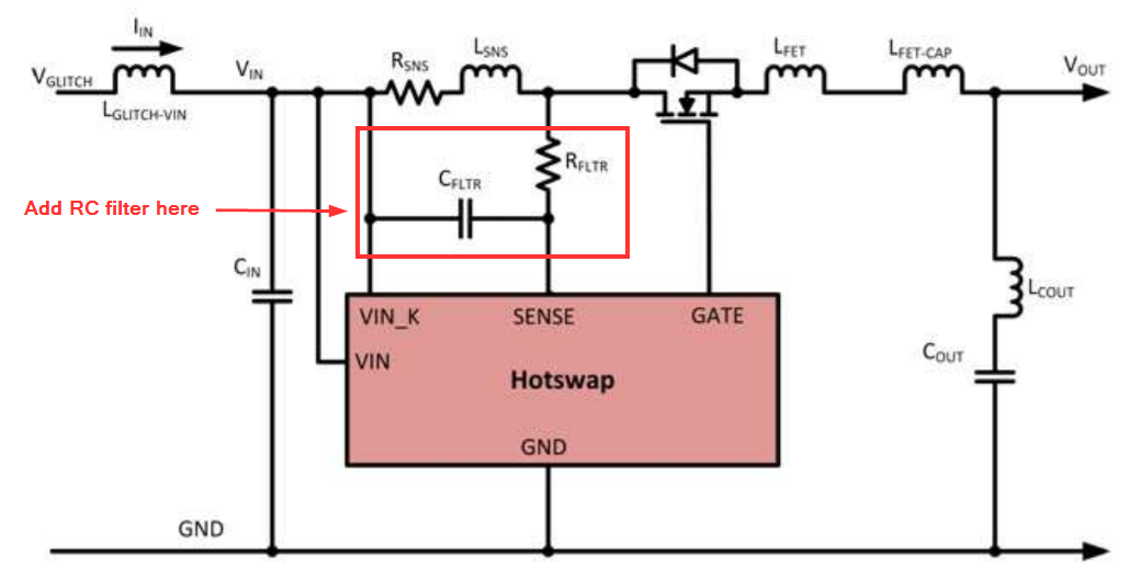
I'm using the TPS2492 as a inrush-current limiter for a DC/DC converter that can be plugged into a supply.

Supply voltage (VIN) is 28 to 42 V.
Total capacitance to be charged is 4000 uF.
Maximum current drawn by the converter is 15 A.

The circuit works well to charge the capacitors at the beginning.

But when the DC/DC converter is enabled, the MOSFET will be turned off immediately.
I don't understand why the TPS2492 switches off the load.
The converter draws only about 1 A at startup.

Here is a measurement:

CH1: input current (at VIN, measure with a current probe)
CH2: FLT_N signal (with pull-up resistor to 3.3 V)
CH3: timer capacitor voltage
CH4: MOSFET gate-source voltage


The VIN and VOUT voltage stays stable when the converter starts.

When I increase the timer capacitor from 3.3 nF to 10 nF, the voltage at this capacitor reaches only 1 V before the MOSFET is switched off.
How could it be that the MOSFET is switched off before the timer capacitor reaches 4 V?

Why will the gate-source voltage of the MOSFET be reduced when starting the converter?
With this low power there should be no power limitation of the MOSFET.

I've attached my excel-calculation.

Any suggestions how to get my system running?


Regards, Florian

TPS249x_8x_Design_Calculator_REV_A.xlsx

  • Hi Florian,

    We try to answer your e2e questions within 24 hours, but because of the holiday season, this might be slightly delayed. I'll get back to you with my comments/feedback/suggestions no later than Friday, but I'm shooting for tomorrow :-) Thanks in advance for your understanding.

    Best Regards,

    Aramis P. Alvarez

  • Hi Florian,

    Let's see if we can solve this issue. Here are some of my comments/suggestions:

    1) There seems to be oscillations/noise on the waveform above, especially on the current itself.  Wires inherently have inductance and the di/dt on the oscillations could be big enough to cause a big differential voltage signal across the VIN and SENSE pins. This will cause nuisance trips (increasing/decreasing gate voltage). The solution might be as simple as adding an RC filter on the sense lines (look below). We have an app note discussing this issue. You can find it at ti.com/hotswap ==> click on the "Technical Documents" tab ==> click on "Handling System Transients in Hot Swap Applications" under the Recommended application notes section. In particular, make sure to read section 3 (page 10) where it talks about the nuisance trips.

    2) After the gate shuts off, there is still current going to the system, by the looks of it on the provided waveform. The FET might be damaged, but I'm not sure. Is the current being measured from the input of the hot-swap controller, before the Rsense resistor? 

    3) I took a look at the calculator tool and noticed that the recommended slew Rate has an N/A for max and min. Usually, on very low SOA margin designs, a dv/dt circuit might not be applicable because the FET might sill be damaged with a phenomenon known as "tail current". I recommend possibly adding a stronger SOA FET, something like the CSD19536KTT will probably be a stronger suited FET for this design.

    4) Would you be able to provide the schematic with all elements connected to our device? Also, if you could provide another waveform probing VIN, VOUT, VGATE, Current IN, and Vtimer, that would be great. If you only have 4 probes, then capture two scope shots, triggering the falling edge of the gate (like in your waveform on top) with the first 4 signals, and then interchanging VIN for Vtimer. The schematic and newly provided waveforms might help us figure out what the issue might be and how to fix it. 

    Florian, please try to implement my first comment and see if that fixes the issue. I'm not sure if it will, but it's worth a shot :-) Thank you for your patience and enjoy your weekend :-)

    Best Regards,

    Aramis P. Alvarez

  • Hi Aramis,

    I'll add my own answers below in blue.


    Best regards, Florian

    Hi Florian,

    Let's see if we can solve this issue. Here are some of my comments/suggestions:

    1) There seems to be oscillations/noise on the waveform above, especially on the current itself.  Wires inherently have inductance and the di/dt on the oscillations could be big enough to cause a big differential voltage signal across the VIN and SENSE pins. This will cause nuisance trips (increasing/decreasing gate voltage). The solution might be as simple as adding an RC filter on the sense lines (look below). We have an app note discussing this issue. You can find it at ti.com/hotswap ==> click on the "Technical Documents" tab ==> click on "Handling System Transients in Hot Swap Applications" under the Recommended application notes section. In particular, make sure to read section 3 (page 10) where it talks about the nuisance trips.

    I'll try your suggestion to damp the ringing. Unfortunately I've no RC filter in my design at the moment. I'll add it when I start the redesign of this board.

    2) After the gate shuts off, there is still current going to the system, by the looks of it on the provided waveform. The FET might be damaged, but I'm not sure. Is the current being measured from the input of the hot-swap controller, before the Rsense resistor? 

    Yes, the current was measured before the sense resistor.


    3) I took a look at the calculator tool and noticed that the recommended slew Rate has an N/A for max and min. Usually, on very low SOA margin designs, a dv/dt circuit might not be applicable because the FET might sill be damaged with a phenomenon known as "tail current". I recommend possibly adding a stronger SOA FET, something like the CSD19536KTT will probably be a stronger suited FET for this design.

    I've seen the suggested MOSFET CSD... before. But I've only space the a DPAK. In the meantime I've found the IPD082N10N3G, which has a slightly better SOA then the IPD034N06N3G. With this one I get a dv/dt value from the calculator.

    4) Would you be able to provide the schematic with all elements connected to our device? Also, if you could provide another waveform probing VIN, VOUT, VGATE, Current IN, and Vtimer, that would be great. If you can only use signals. If you only have 4 probes, then capture two scope shots, triggering the falling edge of the gate (like in your waveform on top) with the first 4 signals, and then interchanging VIN for Vtimer. The schematic and newly provided waveforms might help us figure out what the issue might be and how to fix it. 

    In the first step I'll try your suggestions from above. If I could not get the system running, I'll provide you the additional measurements and an updated schematic.

    Florian, please try to implement my first comment and see if that fixes the issue. I'm not sure if it will, but it's worth a shot :-) Thank you for your patience and enjoy your weekend :-)

    It could take some time for me to give you a feedback, because I've to get the converter running in the near future. Because of that I've tied the TIMER pin of the device to GND to disable the overcurrent protection and use only the inrush-current limiter function.

    Thank you very much for your detailed help!

    Best Regards,

    Aramis P. Alvarez

  • Hi Aramis,

    I've done a redesign of my board:

    • adding a RC-filter at the shunt resistor
    • layout improvements
    • stronger FET

    The inrush-current limiter is now fully working!

    Best regards,

    Florian

  • Hi Florian,

    That's GREAT news! I'm happy to have helped here, and thank you for choosing our part for your project :-)

    Best Regards,

    Aramis P. Alvarez