This thread has been locked.

If you have a related question, please click the "Ask a related question" button in the top right corner. The newly created question will be automatically linked to this question.

TPS61291: TPS61291 high noise while in Step Down mode in range from 3.4-3.9V.

Part Number: TPS61291
Other Parts Discussed in Thread: CC1310, TIDA-00484, TPS63051, TPS82740B

I have a produced board with CC1310 running on 868MHz that uses TPS61291 as the PSU. Board is primarily powered from a LiIon battery pack with its own charging circuit. I used reference design

TIDA-00484  for the PSU. Mean consumption is 10mA with peaks @25mA

RF matching is done with Johanson's balun and a chip antenna is used. SW is Contiki OS. There's a gateway that uses same board.

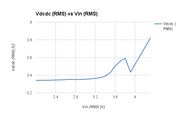
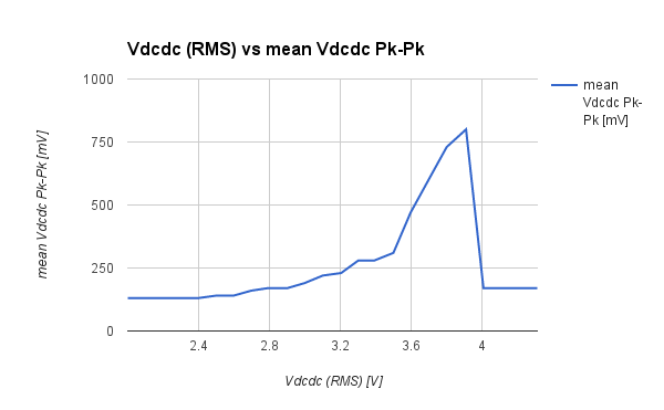
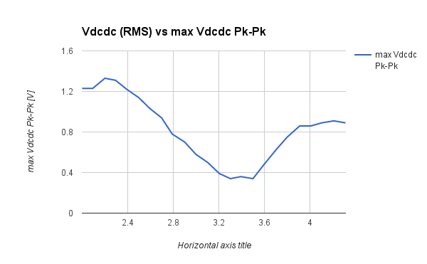
I have an issue running this setup while input voltage is in range 3.4-3.9V. board itself is booting up and operational [I get debug data over UART]. Internal monitoring, ADC, I2C line work fine, but I don't get any transmission out of it. I've tested with a bench PSU over the whole range :


In attached schematic there's a voltage divider. I've tested without it – it doesn't affect the measurements. 

I guess that step down somehow produces a lot of noise with harmonics with enough power to disrupt normal RF operations. This feels like self oscillation to me. 

My question why this happens only in the middle range of the chip voltage and how to fix it. power.pdf

  • Hello
    the TPS61291 is boost converter, which mean the input voltage should be lower than the target output voltage. the output voltage range of a typical 3V~4.2V, which should be higher for the sub-1Ghz device. so you need a buck converter instead of the boost converter TPS61291.
  • Thank you for the reply.
    1. Datasheet for TPS61291 states that input is in range 0.9-5V. Max output is 3.3V, which I expect.
    2. TIDA-00484 uses this IC fro coin cell operations, so I suppose it doesn't represent my case correctly.
    3. I have no problems with TPS61291 when Vin is @ 3.9–4.5V
    4. DO I understand correctly that best option is to have a separate regulator for non–boost operations?
  • the output voltage of the TPS61291 can't be regulated at 3.3V if the VIN is higher than VOUT. And the ripple of TPS61291 would be high at VIN=3.4~3.9V because of this device's operating principle. and at VIN=4.2V condition, the VOUT could reach 3.9 level, higher than voltage of the CC1310 requirement.

    in your application, input voltage is 2.2V~4.2V, and output voltage 3.3V. you need a buck-boost converter TPS63xxx. please start a new post if you need suggestion for buck-boost device.
  • Yes, you have a different battery than the reference design, which has a different voltage range, which requires a different power solution. What voltage range can your loads accept?

    If you must use 3.3V, then the TPS63051 is the best option, as you need a buck-boost converter. However, these do not have ultra-low current consumption like the TPS61291's bypass mode. If this is a concern for your application, you are likely better off with the next option.

    If your loads can accept a lower voltage, like 3V, a buck converter is needed--TPS62740 or TPS82740B. A buck converter can still be used for a 3.3V output, but you won't be able to discharge your battery below 3.3V and keep your system operational. Many customers pick this option, as it is ultra-low power which results in longer runtime (due to higher efficiency) even while leaving some energy in the battery.
  • Thank you all for the reply. Idea was to be able to operate in range of 1.6 –4.5 V on the input and have 3.3 out. Now I understand what confused me so much.  TPS61291 can only operate in bypass mode @3.3V and higher.  I didn't realize that till now – I always struggled with power design.

    I will have to re-think the design now. 

    Strange thing about 3.9–4.2 V operation. Output voltage is very stable @3.6V in that range. 

    Once again many thanks for all the replies.