This thread has been locked.

If you have a related question, please click the "Ask a related question" button in the top right corner. The newly created question will be automatically linked to this question.

TPS61032: TPS61032 Application Help!

Part Number: TPS61032
Other Parts Discussed in Thread: TPS61030, TPS61235P, TPS61236P

Hello, 

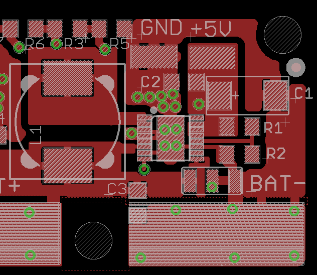
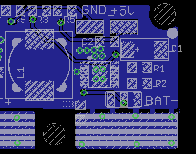
I am trying to create a battery backup system for a raspberry pi model 3.  We are creating a player for digital signage application and knowing common issues of SD card corruption due to power outages.  Anyways the basic circuit is an MCU to manage battery voltage, button interrupts to signal shutdown.  We are using a 400mAH LiFePo4 battery for the backup supply that is charged via microchip's MCP73123.  The basic requirements of the boost circuit is to increase voltage from 3.2 V to 5.1V for the Pi.  Max load current is 1.2A with transients up to 3A.  I have had several of these TPS61032 fail catastrophically (burn up) while in operation.  I'm wondering if someone can point out a fundamental flaw in my circuit design.  Note that the TPS61030 defaults to disabled via a 10k resistor to ground.  The MCU gets power as soon as the Pi is powered via the pi's micro usb power supply.  The MCU first analyzes the battery voltage and enables the boost converter if Vbat is above 3V.  After the boost circuit is enabled the MCU allows the Pi to boot up after Vbat reaches 3.3V.  In the case of a power outage the boost circuit supplies the 5V and the MCU monitors the battery voltage as it drains.  If the Vbat drops below 3.1V the MCU signals the pi to start shutdown.  After the MCU confirms shutdown the MCU disconnects the boost circuit after Vbat reaches 3V to prevent unnecessary drain.  

Thanks!


  • Hello,

    I haven't actually measured the current draw of the raspberry pi 3 running it's application.  The only external peripheral would be the HDMI port feeding video to a TV.  Regardless,  it looks like the Pi 3 consumes a lot more power than its predecessors.  At max CPU load and USB and HDMI peripherals loads can be as high as 2A.  There may also be transient current spikes that are creating problems.  I also noticed the TPS61032 data sheet doesn't mention anything about over current protection.  I think I'm going to chalk this one up to an underrated boost.  With nothing else obvious to me, I have no choice but to look for alternative, perhaps more robust IC's.

    It seems that I should be looking at the TPS61235P device programmed to 5.2V output to provide ~5V through the diode.  This chip boasts some impressive specs 3.3 to 5V conversion up to 3.5A.  Also it has over current protection baked in.

    I would still appreciate any feedback from anyone that cares to share their thoughts.

    Thanks.

  • hello
    i notice you question and will reply next Monday
  • hello
    the damage of boost converter normally be caused by careless layout. the TPS61030 can't support 3.5A output current from 3.1V, its current limit would be triggered. however, this device has current limit function to prevent it from damage at over current condition.

    i would suggest TPS61236P for you application. you can apply an EVM for evaluation, connecting the EVM to the current system board with wires.
  • Jasper,

    Thank you for your reply.  Can you elaborate a little on board layout and what is the common mistake?  I did try to mimic the layout found in the data sheet the best I could.  Note the top layer is red and the bottom layer is blue.  I left the top layer pads showing on the bottom copper image for reference.  Does this look like a bad layout?  What is the reason if so?  Note that the input capacitor C3 is the input capacitor and C1 and C2 are the output capacitors.  C1 is a tantalum capacitor 220uF part# TPSD227K010R0150.  Inductor is 6.8uH 4.9A part # CDRH124NP-6R8MC.

    Thank you.  

  • Jasper,

    I found this excellent write up. e2e.ti.com/.../tips-in-debugging-a-boost-converter . Thanks for writing this up. I know the problem exists across multiple boards so soldering is most likely ruled out. I do know that when the boost circuit fails there is a short circuit from SW pin to ground. This sounds a lot like voltage spikes damaging the internal fet? If I can find some time I will try to capture some waveforms. Would you recommend a tvs diode at the input? In your previous post, are you saying you doubt that over current is the culprit because of over current protection? If so, I tend to agree. To clarify, I expect current draw to be max 1A continuos current not 3.5A.

    Thanks again.
  • 1. the layout is good. and i don't see problem in the external components used.
    2. do you know at which condition the device is easy to damage? the root cause is easy to find if we know the failure condition.
    3. for the failure system board, do they operate well after replacing the damaged TPS61030? i want to check if only TPS61030 is damaged in the system.
    4. the EN of the TPS61030 is controlled by sensing the voltage of the battery from my understanding. do you see high frequency disable/enable signal in the EN pin? high frequency on/off signal is risk to this device.
    5. over current may be an possible root cause. high current causes high voltage spike at the SW pin, which could damage the device. could you try to add snubber circuit at the SW pin according this application note "www.ti.com/.../slva255.pdf"
    6. TVS diode can clamp the over voltage at VIN. have you observed over voltage at VIN? this is possible if the line between the battery the BAT pin is very long. you can try to add TVS or a tantalum capacitor at the input.
  • Jasper,

    1) Great
    2) I do not know the fault condition yet. I do handle these boards and probe them quite a bit as I am testing the board. It may have something to do with programming the MCU / connecting and disconnecting power, or over current. I should be able re-create the condition but it seems a bit random. Some of these circuits have been running for 2 weeks or so. Some fail right away.
    3) After replacing the TPS61030, it functions just fine. Nothing else in the circuit suffers except for a drained battery.
    4) The EN pin is controlled by the MCU and is used very rarely used. There is no condition where it oscillates at any notable frequency. I don't believe this is a problem but the logic level at the EN pin is ~5.1 V but Vbat is 3.3V nominal.
    5) I will definitely try a snubber at the SW node. I will capture the before and after wave forms.
    Nothing else in the circuit is damaged at all. I have seen this on 10+ boards without any other issues. When I replace the boost if functions fine. It seems somewhat random as far as how long the boost runs without issues. I have left a few circuits running for 2 weeks with no issues but one of them was burned up. There is no heat at all from the IC during operation which is not surprising.
    6) I will also try a tvs diode or tantalum capacitor on Vin.

    Thanks