This thread has been locked.

If you have a related question, please click the "Ask a related question" button in the top right corner. The newly created question will be automatically linked to this question.

CCS/BQ24253: Charging problems

Part Number: BQ24253
Other Parts Discussed in Thread: BQ24250

Tool/software: 코드 작성기 스튜디오

Product is being developed using BQ24253.

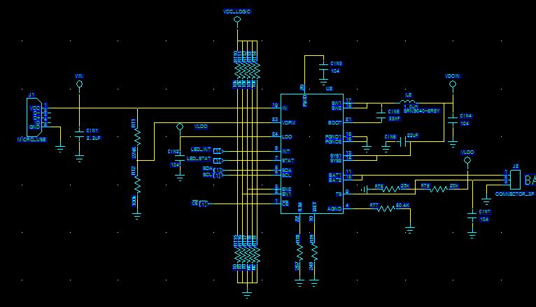
It is composed like the above figure.

The power input is using an adapter(DC5V 2A).

I want to use "externally programmed"(EN2 to 0, EN1 to 1). try to control the current with an external resistor.(current MAX 1.5A). I know that resistors need to be modified.

I am testing, but the charge does not work properly and it flows about 100mA.

Correct the fault in the circuit.

  • Hey stone,

    Do you happen to have a higher resolution screenshot of your schematic? I am having trouble seeing the pull-ups/pull-downs and other resistor values on the part. 

    Just so I'm clear, are you trying to control the input current or the charge current? EN1 and EN2 control the input current limit AFTER D+/D- run detection. This means that EN1 and EN2 need to change to the desired setting after D+/D- detection completes. I cannot see what your ILIM resistor is set to, but perhaps it is the 1.5A max you described in your post. Additionally, if you are correctly setting EN1 = HI and EN2 = LO, then ILIM will be your input current limit. Again, EN1 = HI and EN2 = LO must be set AFTER the detection. 

    Regards,

    Joel H

  • Thanks for the replay.

    I do not speak English well ....
    I want to send a circuit with a high resolution, but I am not very good at PC operation.
    The pull-ups / pull-downs resistors were intended to be designed to use the BQ24250 or BQ24253.

    How long does D + / D- detection time?

    Can you send a reference schematic of BQ24253?

    Korea is an important holiday this weekend.
    I want you to give me a quick answer. I want to solve this problem and relax.
    I ask politely, I do not know if the expression is correct.
  • Hey stone,

    We do not have a direct reference schematic of the bq24253, but we do have a general schematic for our EVM (it assumes the bq24250 is the IC in place).

    See the reference schematic here. This is the bq2425xEVM-150

    There is also a TI-Design using the charger here. You have to select "Download Schematic" and click the Second Link. This will download a zip file with system schematics. You want to open the "2514147E_NIRSCANNANO TIVA BOARD.pdf" where you will also find the bq24250 being used.

    However, both of these will give you a general idea of how to pull-up the EN1 and EN2 pins. 

    The first link is a hardware implementation (you will see D+/E1 and D-/E2 on JP2 and JP5. 

    The second link may be similar to yours, where a logic signal/rail either pulls up the pins or not. Typically I've seen a pull-up either to GND or to a rail, and a some logic switch (like an open-drain/open-collector pin on an MCU). 

    The D+/D- detection can take up to 1sec to allow the charger to connect and detect the host. 

    Figure 18 shows how the bq24253 utilizes the EN1 and EN2 pins after DPDM detection.

    Hope this helps,

    Regards,

    Joel H