This thread has been locked.

If you have a related question, please click the "Ask a related question" button in the top right corner. The newly created question will be automatically linked to this question.

BQ24618: BQ24618 failing over and over...

Part Number: BQ24618

Hello Community,

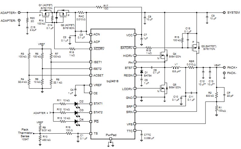
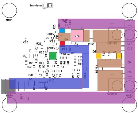
I am having a very bad experiency with the BQ24618. I made a PCB which follows the schematic circuit provided in the datasheet and I have been the most careful possible to meet the layout recommendations. Nevertheless, the charging MOSFETs don't start the proper pwm operation or they even blow-up (specially the low-side MOSFET)

I am using a 3S LiPo Battery and the adapter input voltage is 19V, charging current is 2.8Amps  1.2Amps, precharge current is 10%.... Adapter current regulation is 3Amps 1.5Amps.

I would appreciate any suggestion from those who made the IC to work well... This is the second PCB design we are testing and it doesn' seem to work in any way.

Additional information:

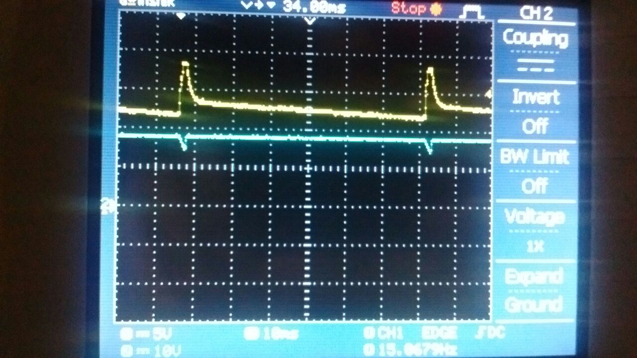
At the beginning, connecting the adapter would make the !PG led to blink at around 11Hz as well the ACDRV and BATDRV (conditions were CE low and Battery absent). The blinking frequency were also dependant of the adapter voltage, oscillating from 10 to 12Hz with Vadpater from 12 to 19V.  Plugging in the battery would make !PG to stop blinking. Making CE to be high would enable REGN to rise at around 6Volts (otherwise it woud remain at low state) But the charging mosfet will never start alternating as the push-pull buck converter they are (just a continuous gate voltage at the high-side) This make PH pin to remain still at +Vbat

Any comments are welcome, thanks in advance!

  • Hi Mauricio,

    I will help you out on this. First please attach the schematic and layout of your design if you can.

    I would check your bench equipment carefully. Make sure there is not a lot of impedance between your power supply and our charger's input. Make sure there is no current limit, which this would cause input voltage to drop, similar to your description.

    Also, can you send waveforms for VCC, VIN, REGN and SRN? Include any conditions which have /PG blinking and conditions where /PG would stop blinking.

    Regards,
    Steven
  • Hi StevenB. Thanks for your attention!

    The schematic is the same as the one provided in the datasheet, just only changing the values of the charge current an ac regulation set resistors. We also added another BATFET in parallel with Q3 to increase the current conduction capability of the circuit (BATTERY-->SYSTEM) The rest is exactly the same:

    This is the layout (some components might have a different reference number in comparison with the schematic showed above)

    • The grey block in the left-bottom corner is the AC adapter (19 Vdc)
    • Green central block is BQ24618
    • Red block is Q4.
    • Light blue block is Q5.
    • Pink block is the inductor (L1)
    • Orange blocks are Q3 and Q6 (Q6 is the additional MOSFET I mentioned above)
    • Light purple path is the Power GND.
    • Light blue path is AC Adapter positive path.
    • Brown path is: the charge path (Q4/5 -> L1 -> RSR1 -> BAT+) and the Bat to system path (Bat+ -> Q3/6 -> Rsys -> System+)
    • Analog groud is in the bottom layer, connected on the BQ24618 thermal pad. Power GND and analog GND are connected together by a single point right next to the thermal pad with a tiny 0 ohm resistor (in the bottom layer).

    The measurements are the following:

    • Vin = 19Vdc (continuous)
    • VCC = same as Vin
    • REGN = 0V (CE low) and REGN = 6.08V (CE high)
    • Vref = 0V (CE low) and Vref = 3,3V (CE high)
    • SRN:   Period: 68ms, Max voltage: 18V; Min voltage 16.7V
    • ACDRV (blue) and BATDRV (yellow):

    Additional information:

    /PG pin will blink with CE high or low and in the conditions measured above. It will only stop blinking when the battery is connected. But connecting the battery will make the AC adpater to supply a current twice the currentset in ISET1, ISET2 or ACSET. When connecting the battery we experienced overheating or destruction of Q4 and/or Q5. We tested another pcb variant with a RC snubber to prevent the accidental triggering of the MOSFETs when inserting the battery, but no improvement was appreciated (we proceeded to continue the tests without this RC snubber circuit)

    We are using a 3S LiPo Battery.

    We have made MANY measurements and tests, we replaced MOSFETS and ICs but the malfunction continues... We carefully followed the layout recommendations as far as possible but we haven't achieved the proper operation of the circuit.

    Our Power supply can deliver up to 3Amps but the AC regulation current is set to only 1.5Amps and the charging current is set to 1.2Amps

    I hope you could guide us out of these problems!

    Thanks in advance,

    Best regards.

    MAURICIO

  • I think I made it work. For some reason, the previous high-side MOSFET was bad. So I tried new MOSFETs and I added a slightly bigger gate resistor. This time they managed to charge the battery! but I am not completely sure about the triggering of the gates (regardless the IC did charge the battery): 

    High and low side MOSFET of the Buck Converter

    The yellow curve is the High-side MOSFET's gate voltage. Bootstrap make it 6V above the source voltage, this works great. But the blue curve is the low-side MOSFET's gate voltage. The ugly shape of low-side gate right after the triggering is due to some poor response of my oscilloscope's channel 2 (it would look much better if I measure that gate with channel 1 only) My question now is: Why low-side gate is only triggered for a short while and not along all the low-state of the high-side MOSFET?

    I expected a push-pull alternating triggering.

    Vin voltage is 18,4V and battery voltage is around 11,8V (not fully charged). Charging current is set to be 1,2Amps.

    Best Regards

  • Hi Mauricio,

    It looks like it is running in non-synchronous mode, but that mode only happens if your charge current is below 0.5A, or forced if SRP-SRN is 1.25mV. Can you measure how much is your SRP-SRN voltage? Also if you have a current probe on the scope, try to plot current of the inductor by lifting the inductor and using a wire to connect it.

    What was the previous MOSFET you used and which one is the one that fixed the problem? Send a schematic even though you mention it looks similar to our datasheet's schematic. There might be something with the components selected.

    For the scope shot, send a clear waveform for HIDRV, LODRV and PH. Use the GND closest to the test point and try using the smallest cable possible to connect to GND. If you shorten the loop, there shouldn't be that much noise in the waveform.

    Regards,

    Steven