This thread has been locked.

If you have a related question, please click the "Ask a related question" button in the top right corner. The newly created question will be automatically linked to this question.

TPS55340 Based Flyback - Very Poor Load Regulation

Other Parts Discussed in Thread: TL431, TLV431, TPS55340

Hello everyone,


I am trying to replicate the 5V, 2.5A DC-DC flyback converter as seen in this evaluation board: http://www.ti.com/tool/tps55340evm-148

My specifications are as follows:

  Vin: 10V to 14V

  Vout: 5V

  Iout: 2.5A

As compared to the eval board, I have made the following modifications in my circuit:

  1. Changed TLV431 (Vref = 1.25V) to TL431 (Vref = 2.5V).  I have made changes to the voltage divider on the REF pin of the TL431.  These resistors (R8 and R14) in my circuit are 4.7K and 4.7K.

  2. I have temporarily removed D3, R6 and C18, which is the secondary side soft start circuit.

  3. I am using the optocoupler PC817 instead of the TCMT1107 used in the eval board.

  4. I am using a self assembled transformer instead of the Coilcraft part used in the eval board.  Details of the transformer given below:

           Core type: EE

           Core center limb breadth, width: 5 mm

            Core height: 10 mm

             Lprim : 1.66 uH

             Nprim : 9 turns

             Nsec : 5 turns

Problems I am facing:

  1. Output voltage drops from 4.94V to 2.2V when I load the circuit with a 25 Ohms resistor.

  2. Switching frequency is around 87 KHz which is 1/4th of the desired switching frequency of 350 KHz.  (Frequency foldback feature showing collapsed output.)

  3. Optocoupler does not turn on (no current seen through the resistor which is in series with optocoupler diode (R9)).

  4. Voltage at cathode of TL431 is 4.1V.

I don't know why the controller is operating in frequency foldback.  This feature is supposed to be active only in case of over current protection.

Please help.  Thanks for your time and effort in advance.

With regards.


  • Hi,

    I think this post is in the wrong forum, I will move it to the correct forum and alert the applications team to respond to your questions.

    Regards

    Peter
  • Hi,

    There are a lot of variables here so I suggest trying these changes, one at a time, to limit them and fine what one is causing the issue. For example I suggest the following based on the changes described. 2-5 probably do not have to be in any particular order.

    1. If you aren't already, I suggest testing on the EVM (if possible with the transformer) to rule out PCB layout
    2. Change to the TLV431 circuit
    3. Change the optocoupler
    4. Remove the secondary SS circuit
    5. Change the transformer

    Hope this helps.

    Best Regards,
    Anthony

  • Hello Anthony,

    It's really good to see a reply from you. Since you were the author of the App. Note, I was hoping to reach you and ask my queries (I even sent a Linked-In request.) Pleasantly surprised to see your reply on this forum.

    My replies:

    1. I am about to purchase the EVM and all the critical parts you mention (transformer, optocoupler and TLV431).

    2. Would like to know if the TL431 is absolutely unworkable. I had used the TL431 because the TLV431 is not locally/readily available. Could you please give me a hint of the calculation involved in selecting the TLV431 and not using the TL431. I tried setting the output voltage for the TL431 to 3.5V in the TL431 spreadsheet calculator that is available here: www.ti.com/.../TL431CALC. The reason for using 3.5V was to turn on the optocoupler diode with the voltage differential between the supply output voltage (5V) and the TL431 output voltage (3.5V), (thus giving a voltage of 1.5V across the optocoupler diode). I found that the values calculated by TL431 spreadsheet don't work either and the optocoupler does not turn on.

    3. Once again, would like to know if there is critical dependence on the optocoupler CTR? (I thought if the TL431 works, the PC817 should be fine.)

    4. Yes, I am testing without the secondary side soft start.

    5. Yes, will try with the transformer used in the EVM.

    Once again, thanks for taking the time to reply. I hope to see your reply and check where I am making a mistake in my debug. Will definately implement your suggestions.

    With regards.
  • Glad to help and to see you've read the app note!

    For the TL431, I have tested with this before with no issue. One key thing when making this change to limit the impact on the control loop is you will want to keep the upper resistor in to the REF pin (R8) is kept the same. To minimize the impact of changing to the TL431, the output voltage should be varied by changing the bottom resistor (R14) only.

    For the opto, I would only expect a different CTR cause an issue if the change in gain caused an instability in the loop. If you'd like to take loop stability out as a factor you can try changing the compensation on the COMP pin to 150 ohm and 1 µF. This change will reduce the gain of the loop by a factor of 10 or by -20 dB.

    My original suspicion is this related to layout so I believe you'll make some good progress to figure out the problem after you get an EVM.

  • Hi,

    I just wanted to post in this thread because I am seeing a very similar issue.

    I am using the TPS55340 as a non-isolated flyback regulator to generate +/-15 V. I didn't base my design off the eval board. My feedback purely comes as a voltage divider from the 15 V rail to ground. My -15 V is unregulated (no feedback). There is no isolation in the feedback loop. It is merely two resistors between FB, +15 V, and GND.

    My specs:

    Vin: 5 V

    Vout: Two phases: +15/-15 V

    Iout: 60 mA

    Fsw: 100 kHz (I've also tried 150 kHz)

    Css: 47 nF

    When I apply a very small load to each phase (5 mA), I get +15/-15 V as expected.

    When I start to go much above 10 mA, the load starts to drop in voltage. I get somewhere between +/- 10 V and +/- 14 V depending on the load. The DC voltage on the feedback pin tracks my output voltage as expected. Also of note the voltage seems mostly stable even at these low voltages: 50 mV of ripple or so.

    I've played around with the compensation quite a bit with no luck.

    Eventually, I went ahead and added a 100 nF capacitor to ground on my FB node, which should drastically cut down loop bandwidth, but should make the loop stable. This experiment didn't make any difference, suggesting that compensation is unlikely to be the issue.

    I've taken some measurements, and I have a couple observations:

    1. When the device is operating properly (light load), the SS pin reaches 2.3 V. However, when the device is operating improperly (high load), the SS pin only gets up to 1.2 V. I measured the SS rise waveform, and I can see that when the device is enabled, the SS pin gets up to about 1.5 V, and then falls to 1.2 V about 50 ms after the device is enabled. It remains at 1.2 V until you power off the device.

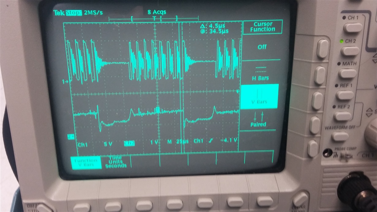
    2. When the device is operating properly with a light DC load, the COMP pin is very stable (as expected). However, when I apply a higher DC load, the COMP pin behaves strangely, and therefore pulses are skipped. The COMP pins seems to get up to about 1.7 V, and then it suddenly drops. This seems to make sense as the SS pin is still at 1.2 V and there is apparently a BJT transistor between the two pins.

    Here's a photo of the COMP pin (trace 2) and switching node (trace 1) when the device is not working properly. You can see that "pulse skipping" occurs, even though I am nowhere near the minimum ontime of 77 ns.

    My primary inductance is 9.9 uH. I wouldn't really expect more than about 2 amps in this application through the primary winding, so I don't think I'm reaching a current limit.

    Any insights would be appreciated. I can provide more details as needed.

    Thanks,

    Matt

  • Hello Anthony,


    Thanks for your second reply.  I will be receiving the EVM board in some time (it has to go through an import procedure).  Until then, request you to please post the values of the control loop; ESPECIALLY the voltage divider resistors on the REF pin of the TL431.  My specs are given in my first post and are similar to the specs of the EVM board.  What would be of greater help is also the outline (if not the details) of the calculations used to arrive at these resistor values.

    I agree, it could be a layout issue.  The tricky part with layout issues is that you never know until you respin the board.

    Also, it would be good to read your replies on 's post on his TPS55340 based "non-isolated flyback".

    Thanks for your time.  With regards.

  • The application note gives details on how the values were selected for the EVM design. Check out sections 2.10 to 2.12. I've linked it below for quick access as I know you already read it.

    For Matthew's case, it may also be layout related since he already tried slowing down the loop. However instead of adding capacitance to FB, the suggested way to slow down the loop response is to increase the capacitance and decrease the resistance connected from COMP to GND. This is where the 150 Ω resistor and 1 µF capacitor suggestion will work. If the issue persists, this will rule out the loop stability as the cause of the issue.

    Matthew, based on SS dropping it sounds like your issue may be related to the TPS55340 shutting down. The SS pin is only discharged of the IC is disabled. Can you check to make sure VIN and EN are not dropping for some reason in your testing?

    I also suggest checking to make sure your PCB layout follows our datasheet recommendations and looks similar to what was done on the EVM. Amongst other things, there are three key ones below to make sure of.

    1. The loop created by the ceramic input bypass capacitors, primary winding of the transformer and internal low-side MOSFET of the TPS55340 must be kept as small as possible. The traces connecting them should be as wide as possible. Preferably the routing in this loop should be done with a copper pour, not a small trace.
    2. Use separate AGND and PGND regions in the layout. Connect them together in only one place to minimize circulating current and make sure there is not any added noise in the analog control circuit. It is recommended to make this connection by connecting the AGND pin directly to the thermal pad beneath the IC.
    3. Follow the guidelines in the datasheet for which components need to be connected to AGND.

  • Hi Anthony,

    Your post helped me solve my issue, so I wanted to post what fixed it for me:

    My layout was as per the datasheet suggestions (and as per your suggestions above) in all ways except one: the ground connection between my ceramic input capacitor (right at the VIN pin) and AGND of the device of the device was very "long". I had cut the ground plane in a bad place, which made the loop very long.

    To fix it, I bridged the cut with a mere 30 gauge wire, and this made the controller work reliably. I've since upgraded my 30 gauge wire to something bigger, and it still works well.

    Thank you again for your help!

    Matt

  • Hi Matt,

    Thanks for the update. I'm glad to see you got it working.

    Best Regards,
    Anthony