


Hi team,
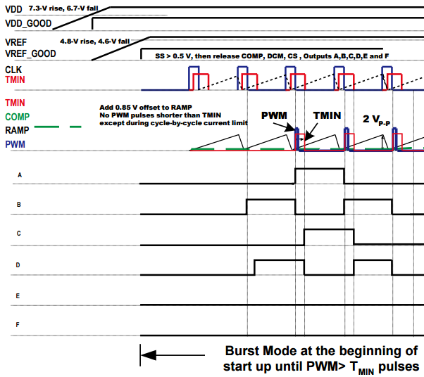
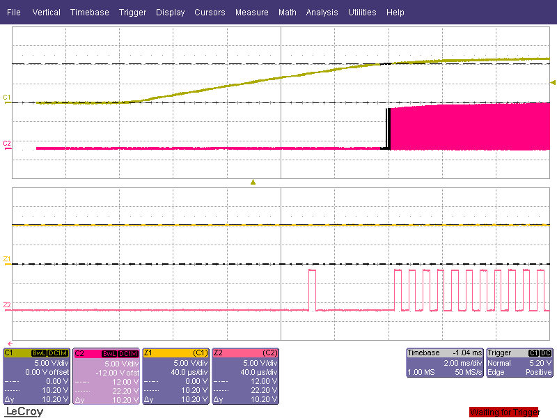
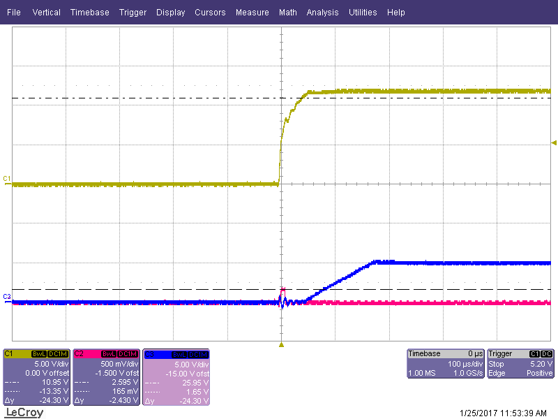
What is the duration time from VDD applied untill OUTx are fixed to low?
We presume those pins are high impedance for a certain period (eg, before VREF starts), is this assumption correct?
This is needed for designing.
Hi team,
What is the duration time from VDD applied untill OUTx are fixed to low?
We presume those pins are high impedance for a certain period (eg, before VREF starts), is this assumption correct?
This is needed for designing.


