This thread has been locked.

If you have a related question, please click the "Ask a related question" button in the top right corner. The newly created question will be automatically linked to this question.

TPS40210: TPS40210 is not working

Part Number: TPS40210
Other Parts Discussed in Thread: TINA-TI

Hello All,

My design parameters are as below.

Input voltage = 12V

Output voltage = 92V

Output Current = 0.1A

Below is the WEBENCH design for TPS40210 that I got from WEBENCH Designer Tool.

TPS40210_92V.pdf

My hardware design is same as WEBENCH design except below components.

Cin = 10uF

Cbyp = 100nF

M1 =  IPP530N15N3 G 

D1 = RR2L4STE25

Cout = 47uF

Coutx = 100nF

But It is not working.

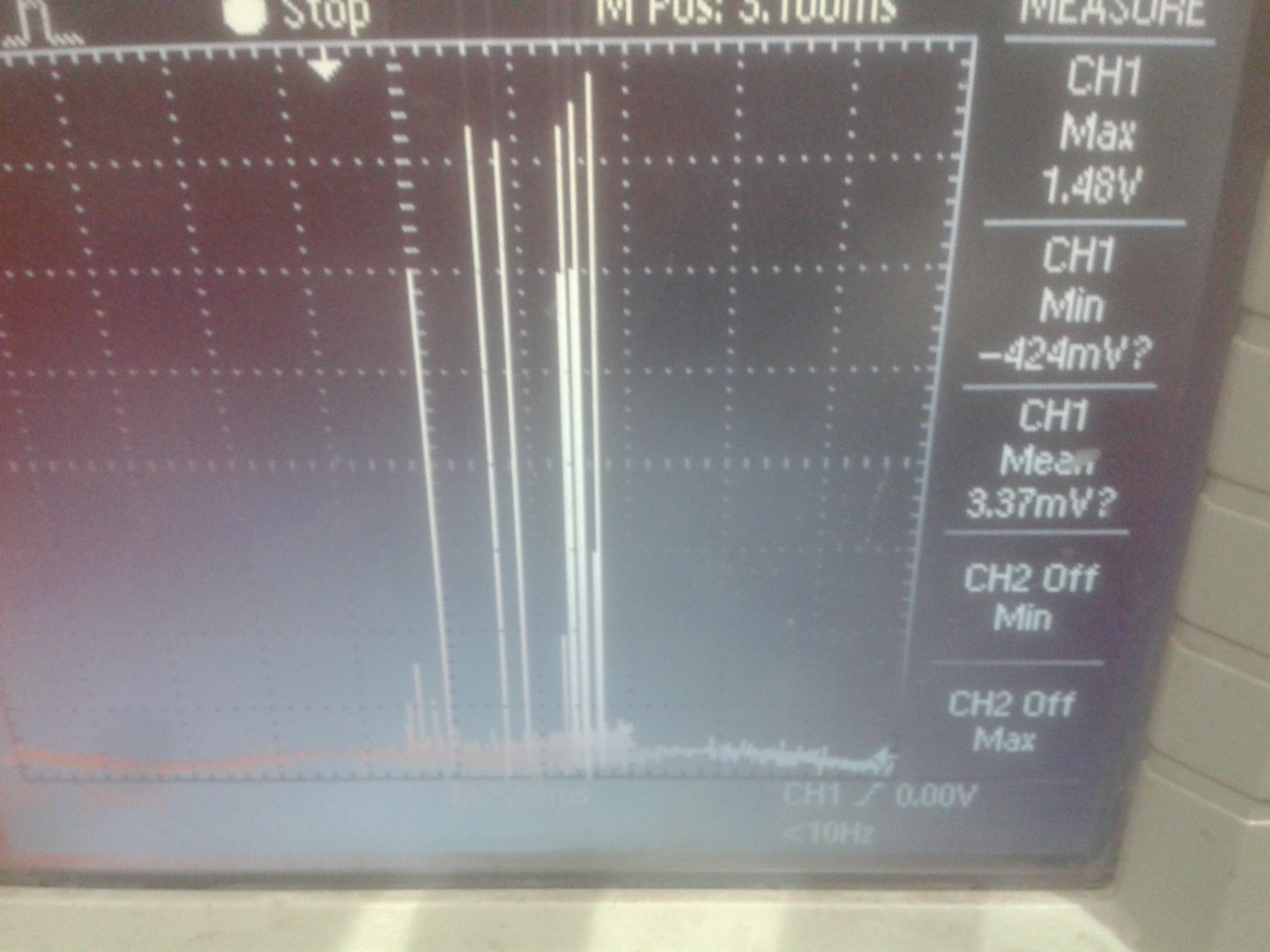
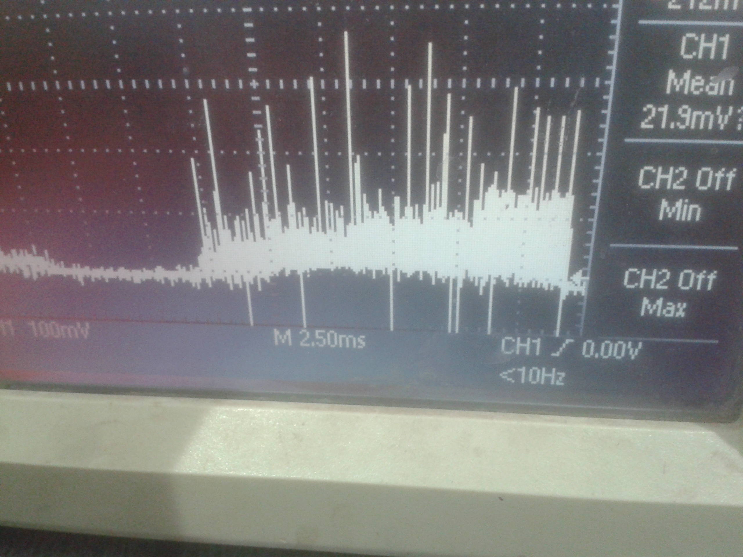
My output voltage is continuous varying between 15V to 23V instead of stable 92V.

Vout is switched using NPN ransistor through 5K resistor. But currently it is off. So, vout is currently at no load.

I tried to simulate the design in TINA-TI. but I found operating point error.

I do not know how to solve it.

Below is the TINA-TI Design file.

TPS_40210.TSC

Kindly help me to solve below problem.

what is wrong in TINA-TI design simulation.

why I do not get 92 stable voltage?

Regards,

Jigar Patel

  • Hi Jigar,

    Can you provide the Vout and GDRV waveforms?
    Can you check if TPS40210 power pad is well connected to the ground?

    Thanks
    Qian
  • Hi Qian,

    Thanks for your replay.

    I have made design from WEBENCH Designer Tool.

    I get  some strange response.

    For same parameters,(Vin  = 12V, Vout = 90V, Iout = 100mA)

    I get  two different design from WEBENCH Designer Tool.

    PFA below design reports.

    TPS40210_90V_OLD.pdf

    TPS40210_90V_NEW.pdf

    I have selected TPS40210_90V_NEW design for hardware making because I doubt on TPS40210_90V_OLD design.

     
    Components which are differ from WEBENCH design as below. 
    Their specification match with WEBENCH components.
    MOSFET M1 = IPP530N15N3 G
    Diode D1 = RR2L4STE25


    When I checked practically on hardware PCB, output voltage is fluctuating from 12V to 15V.
    Oscillator is working properly that I have checked.

    Then I changed output parameters(Vin  = 12V, Vout = 92V, Iout = 100mA) to remove two design confusion.
    PFA below design report.

    When I checked practically on hardware PCB, output voltage is fluctuating from 12V to 23V.
    Oscillator is working properly that I have checked.
    What the problem is at overcurrent protection side. 
    IC shutdown due to overcurrent until SS cap discharge. Then it is restart again.
    This cycle repeats continuously.
    If I short current sense resistor (Rsense = 75mOHM), then I get the output voltage to 91.5V.
    But it is not proper solution. isn't it?
    PFA below ISNS pin voltage & voltage at current sense resistor pics from Oscilloscope.
    can you tell me what was wrong with my TINA-TI simulation design?
    Kindly, help me to solve the issue !!!

    Regards,

    Jigar Patel

  • Hi Jigar,

    Is ISNS cap (Ciflt) close to the ISNS pin in layout? Where is this cap grounded?
    Can you check if there is large noise on ISNS pin?
    If that's the case, can you try to increase Riflt value to see if it helps to solve the issue?


    Thanks
    Qian
  • Hi, Qian

    PFA voltage booster schematic portion of my hardware PCB.

    SCHEMATIC1 _ Voltage_Booster_Circuit.pdf

    PFA placement pic of my hardware PCB.

    PFA layout pics of my hardware PCB.

    I will increase Rifit & will let you know about the result.

    Regards,

    Jigar Patel

  • Hi,Qian

    I have increased Riflt from 1K to 4.7K. 

    same problem is coming but output voltage fluctuation is increased to (12V to 52V) instead of (12V to 23V). (noise level decreased then previous.)

    Then i have tried 10K instead of 4.7K.

    but result is same as 4.7K. 

    PFA pic of voltage at current sense resistor(Rsense).

    PFA pic of voltage at ISNS pin.

    Regards,

    Jigar Patel

  • Hi Jigar,

    Based on calculation, Tss=41ms.

    The charging current is Vout*Cout/Tss=0.105A. If there is 0.1A load current, the total current should be 0.2A.

    Considering the variation of OC threshold, L, Cout and other components value, the sensing resistor value might be too large.

    Can you reduce sensing resistor value to half (37.5mohm) and try again?

    If the problem still exist, can you short ISNS pin to ground and measure the voltage across sensing resistor during soft start and stead state?

    This give us an idea if the voltage across sensing resistor is beyond OC threshold.

    You might need to add another RC filter (like R91 and C97 in your design) and measure the voltage across capacitor during measurement, because there is high voltage noise across sensing resistor.

    Thanks

    Qian

  • Hi Qian,

    I have reduced current sense resistor to 37.5mohm, but when I powered on my circuit, smoke was coming out from inductor in the circuit.

    I immediately turn off power. when i checked MOSFET, It was damaged ( Heatsink is already attached with MOSFET).

    I have replaced MOSFET, INDUCTOR with new one but now output voltage is only 12V. I am afraid that IC has been damaged.

    Then

    I have taken another board &  open R91 ( series resistor in RC filter).

    I have pull down ISNS pin to ground with 1K resistor.

    Currently current sense resistor is 75mOHM.

    when I power on the circuit, some kind of noise(voice pulse) come from inductor (this voice comes only one time during power on, then it is disappeared) & output voltage comes 93V stable without fluctuation.

    PFA pic of voltage at current sense resistor(75mOHM) during start up.

    PFA pics of voltage at current sense resistor(75mOHM) at steady state after power up.

    Regards,

    Jigar Patel

  • Hi Jipar,

    Looks like there is very high noise on R92.

    Can you keep R91 open, pull ISNS pin to ground with 10k resistor, and measure if there is high noise on ISNS pin. Just want to check if there is noise coupling from SW to ISNS pin. Please put the probe ground close to TPS40210 GND pin (pin 6) during measurement.

    Also, can you try below method to see if they help to reduce the noise on R92.

    • increase R90 value, this is to slow down the turn-on of Q2, hence to reduce the noise on R92.
    • Add RC snubber in parallel with D10.
    • Add more ceramic cap on output (close to D10).

    Thanks

    Qian

  • Hi Qian,

    Can you keep R91 open, pull ISNS pin to ground with 10k resistor, and measure if there is high noise on ISNS pin. Just want to check if there is noise coupling from SW to ISNS pin

    I have done this, but there is no noise on ISNS pin.

    My PCB has been damaged due to soldering desoldering process. So I have to make new PCB.

    It will take some days due to components procurement. I will get back to you after few days.

    Sorry for this delay!!!

    Regards,

    Jigar Patel

  • Hi Qian,

    I have made Switcher Pro design on my PCB with same input & output power specs.

    PFA switcher pro design.

    TPS40210_92V_SwitcherPro.pdf

    And finally it is working well without any issue.

    I cant find what was wrong with WEBENCH design.

    Thanks for your support.

    Regards,

    Jigar Patel

  • Make sure to save your Switcherpro documentation. Online Switcherpro is being discontinued. User design information and created designs that are not downloaded before May 2, 2017, will be lost.