This thread has been locked.

If you have a related question, please click the "
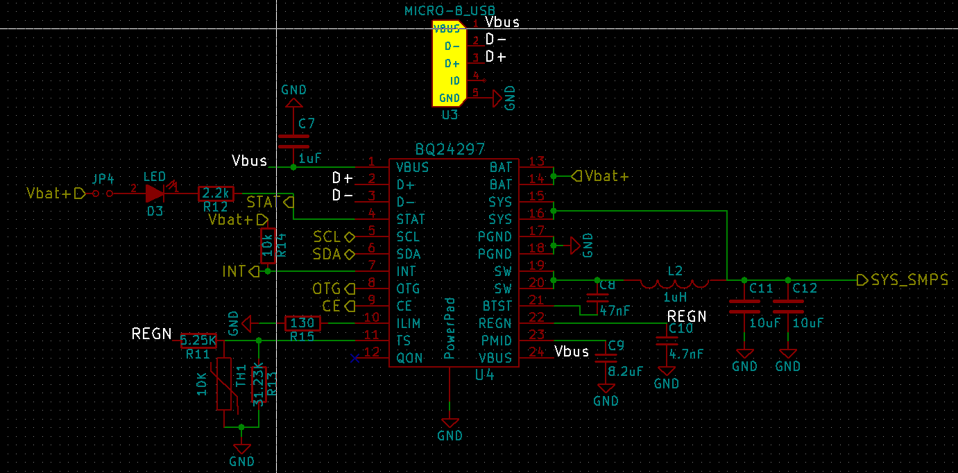
Ask a related question" button in the top right corner. The newly created question will be automatically linked to this question.

BQ24297: Schematic Check

Part Number: BQ24297

I've designed a charging circuit using the application schematic in the datasheet using the BQ24297, I'd just like a second opinion to make sure that I understood everything correctly and it will work. (MAX Charge Current = 3A) **(also note that  pull ups on SDA/SCL are present elsewhere in the circuit) 

Thank you! 

  • Hello Samuel,

    See my comments below:

    • The capacitance on REGN must be 4.7uF instead of 4.7nF.
    • Add a pull-down on CE such that there is a fixed logic state on the pin at all times
    • Add a pull-up on OTG such that there is a fixed logic state if OTG is intended to be used.
    • The pull-ups for STAT, INT I suggest connecting them to SYS instead of directly to BAT.
    • I recommend adding a 0Ohms resistor in series with the bootstrap cap to have the footprint of a snubber resistor in the event slew rate wants to be modified.
    • Also we recommend to add an additional X7R 1nF decoupling cap on PMID and SYS to improve EMI performance. An additional optional 1nF can also be added on VBUS and BAT to further improve EMI.

    Hope this helps.