This thread has been locked.

If you have a related question, please click the "Ask a related question" button in the top right corner. The newly created question will be automatically linked to this question.

BQ34Z100-G1: Programming .srec / .dfi files using custom software tool

Part Number: BQ34Z100-G1
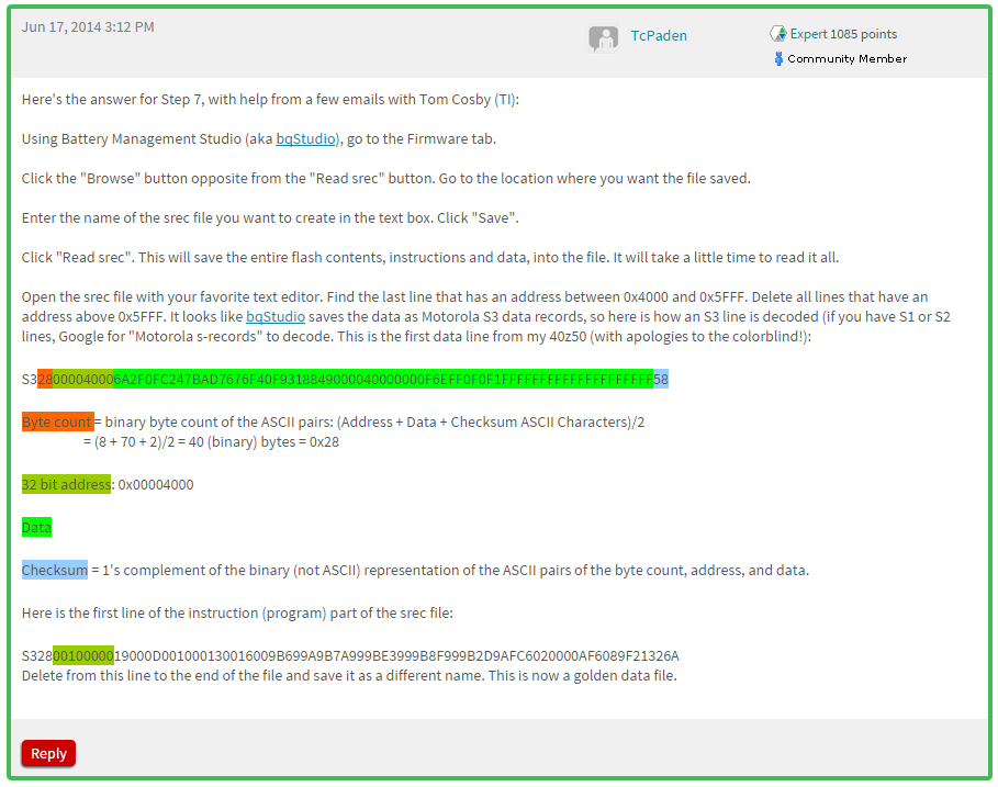
Other Parts Discussed in Thread: BQ34Z100

Hi,

We are looking to automate programming the .srec/.dfi files using our own tool.  Is it possible if you could provide

the file format of the .srec/.dfi files?  Do you happen to have any existing procedures or documents showing how to

program these files?

Thanks,

-Andy

  • Please checkout SLUA665.

  • Hi Damian,

    Thanks for the reply and information. I did go over the document and I also went through the Visual Basic codes,
    but I was hoping if you have any information with regard to the .srec and .dfi format? It would be helpful if there is
    any formal documentation on the .srec and .dfi format, and once I know the format, I can custom our software tool
    based on our specific needs. I also would like to know how to perform checksum or any type of error checking on
    the .srec and .dfi files.
    Going over the Visual Basic codes probably not the best way for me to understand the file format, since I am not
    really proficient in Visual Basic, and going over the codes could take quite a long time which my management may
    not allow me to.

    Thanks,
    -Andy
  • Hi Andy,

    SREC is based on Motorola S-record standard. You can find this info on the web. Here's a screenshot of a previous E2E post.

  • Hi Damian,
    Thanks for the information. I would like to ask a few more questions for my own clarification.

    32-bit address: what would be the meaning of this address field? Is it related to the target register address of the slave device address?
    Data: as for the data field, does it mean that I can blindly write to the I2C bus the actual ASCII data as seen?

    For example, one of the line of my .srec file is:
    S31A 00004015 520921326D00000000D07E17DF000017F300003A36 B7

    The 32bit address is: 00004015
    The data field is: 520921326D00000000D07E17DF000017F300003A36

    In I2C, I would have to follow this format: [slave address][starting register][actual data].
    How would I translate the line above into the I2C format?

    Thanks,
    -Andy
  • Hi Damian,

    OK, I've done a bit more research and here is what I can provide what I know now.

    Based on this link from Thomas, /cfs-file/__key/communityserver-discussions-components-files/196/8360.6215.Bq40z50-Data-Memory-Programming-for-Mass-Production.pdf, I was able to understand a bit more the register addressing scheme.

    Please correct me if I am wrong, since it will help us getting our automated tool working.

    The BQ34Z100 data register for the .srec file starts at 0x4000 and based on your post, stops at 0x5FFF.

    The instructions register starts at 0x100000 which should be ignore.

    For example, my .srec file goes something like this:

    S00F00004657303130305F30305F31360D
    S31A00004000831878C2972D7A96FA99F60C0000934651F6C9F41476
    S31A00004015520921326D00000000D07E17DF000017F300003A36B7
    S31A0000402AFD910025300100EF0511050100001001003C00503CB3
    S31A0000403F00643C00200BB00000021069FED5FB950002001403F4
    S31A00004054E8030001F4001E003C0E10000A46051E030F03200051

    ........

    S31A000043C601A5FFFFFE59FFFFFFFFFFFFFFFFFFFFFFFFFFFFFFF0
    S31A000043DBFFFFFFFFFFFFFFFFFFFFFFFFFFFFFFFFFFFFFFFFFFDC
    S315000043F0FFFFFFFFFFFFFFFFFFFFFFFFFFFFFFFFC7

    .........
    S31A001000000033FFEA0033FAB10033FB6C0033FE950033FEAD009D
    S31A00100015155454003FFFFF003FFFFF003FFFFF003FFFFF003FD0

    ..

    First the line staring S0 should be ignored since it's the header usage only?

    I should ignore everything after S31A00100000 correct since these are for the instruction registers?

    My other question is to write to the register starting at 0x4000 I need to use the command 0x44 correct?

    Thanks,

    -Andy

  • Hi Damian,
    Actually I found that the device BQ34Z100 is a little bit different. The data flash access is organized in SubClass, Offset,
    therefore I cannot do a straight write based on the S3 data format. I need to map the S3 format into Subclass/offset
    according to the BQ34Z100 format.
    For example, given

    S31A00004000831878C2972D7A96FA99F60C0000934651F6C9F41476
    S31A00004015520921326D00000000D07E17DF000017F300003A36B7

    The register address is: 0x4000
    Data is: 0x831878C2972D7A96FA99F60C0000934651F6C9F414
    How do I map this to the BQ34Z100 subclass/offset?

    Thanks,
    -Andy