This thread has been locked.

If you have a related question, please click the "Ask a related question" button in the top right corner. The newly created question will be automatically linked to this question.

CCS/BQ76PL455EVM: Sample code for TMS57004 and BQ76PL455EVM not working

Part Number: BQ76PL455EVM
Other Parts Discussed in Thread: BQ76PL455A, BQ76PL455A-Q1, EM1402EVM

Tool/software: Code Composer Studio

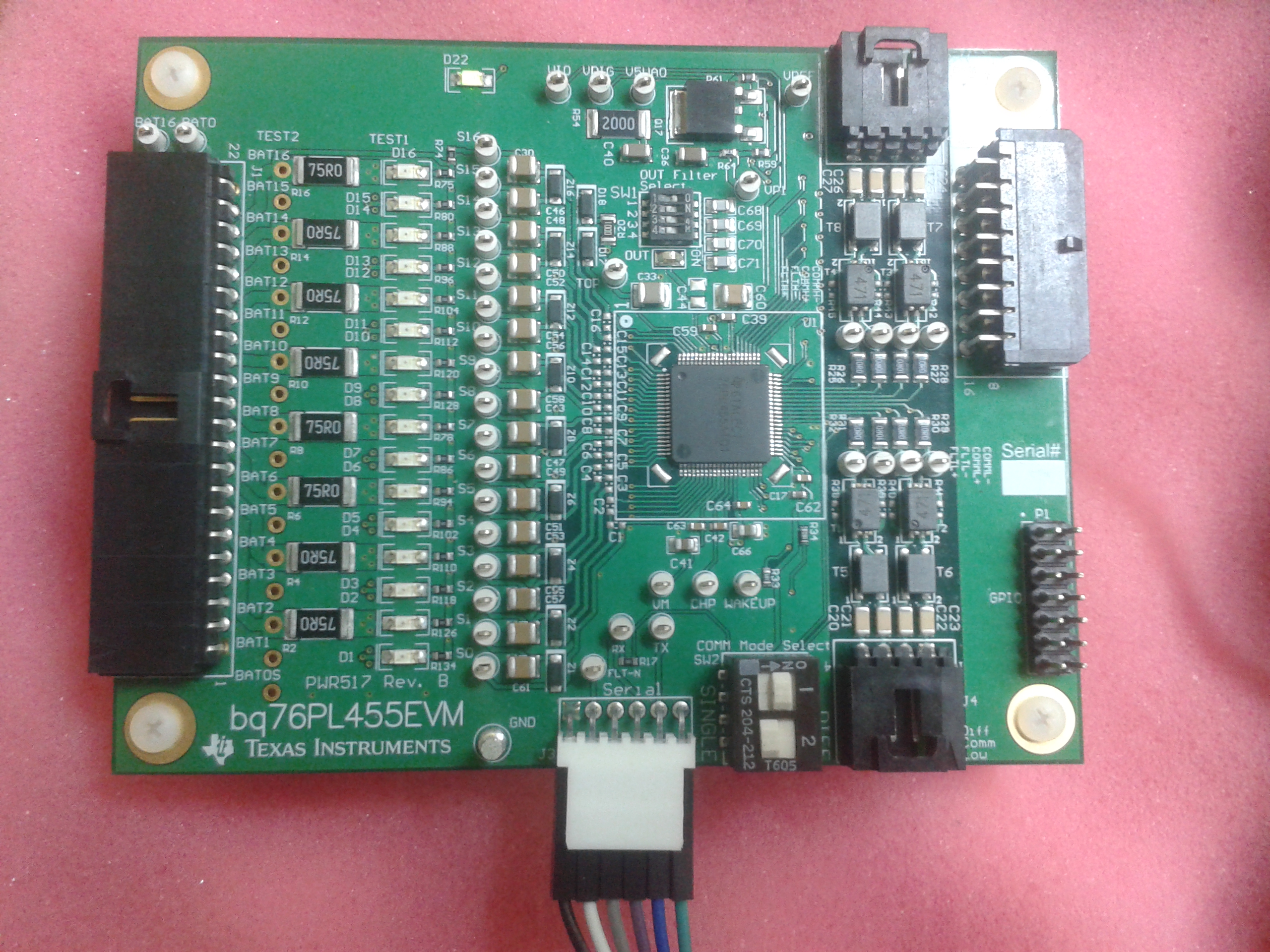
Hi good day, I am trying to program the TMS57004 Launchpad with the sample code provided by TI to work with the BQ76PL455EVM. I have removed resistor R8 as was stated in the code heading.

Is the sample code provided able to work as is or does some modification need to be done?

  • Hi  Ruby,

    The sample code is intended to "work" as-is, but is  not useful. The code is mostly examples of  configuring registers. Have you looked to see if there  is any communication back to the MCU on the RX line? 

    I just hooked up an EVM to a TMS570, and used  a Saleae Logic Analyzer to verify that it should upload as-is. You can  see that  the 455 EVM receives a string  of commands on the RX line after the wake tone, and sends packets back on the TX line when a  response is requested:

  • Thank you for your response, I tried connecting it and connected the rx, tx and wakeup pin using a TDS2000C Digital Storage Oscilloscope and did not receive any output on these pins. However, when i try it with the GUI I receive output on the pins. Can you give me the steps you took in a little more detail please?
  • Ruby,

    No problem...

    Starting  with the bq76PL455EVM....

    1. Set the  switches  SW1 and  SW2.
      1. SW1  should be switched towards  the side  with the  text that reads "1234"
      2. SW2 should be  switched  towards "Single",  since you are not using the isolated  comms
    2. The  bq76PL455A is  powered off  of the battery stack. With the bq76PL455 EVM, we can simulate the battery voltages by taking a power supply and using a simple resistor ladder to  mimic the voltage drop of a cell. The 455 needs a minimum of 12V at the top of the stack to work. In our lab we use  sixteen 100 Ohm  resistors in series, and connect the 455 to each  tap. Connecting  a  power supply to this resistor divider should work all the way down to ~12V.  If  you  don't want to get into high voltage, I  suggest using something like 20V. This will create a cell undervoltage fault condition  with the default settings, I believe. This  would  only cause the  nFault pin to trigger, though. 

    Time for the  MCU...

    1. Connect the MCU header pins  to  the header J3 of the 455 EVM
      1. These connections are detailed at the beginning  of the  sys_main.c file.
    2. Assuming  the project has  been imported into CCS and  compiled, connect the MCU to the PC w/ the USB cable
    3. Build the project in CCS
    4. Run the debugger, and  hit Resume (F8). This  runs the code on the  microcontroller, and will allow you to step through the code and hit breakpoints.

    I also apologize - in my earlier reply i had  forgotten to remove  resistor R8 of the MCU. After doing so, the responses should look like this:

  • Thanks again David.

    Is there any "useful" code available to program the TMS57004 to control the bq76PL455EVM?


    Regards,

  • Hi Ruby,

    Unfortunately, we do not have any code published that is "plug and play", mostly for liability reasons. However, the example code will work well as skeleton code. The commands are already built in, it is just up to the user to decide how to use them.

  • Thanks again David.

    I tried connecting the MCU to the EVM again and following the instructions that you outlined after "Time for MCU".
    The JTAG LED (D8) blinks when I step through the code which I interprete as communication between CCS and the MCU.
    However, after stepping through the entire code, neither the SCI1TX (D5) or SCI1RX (D6) on the MCU blink and there is no output on the wakeup, RX or TX pins on the EVM.
    Aren't the SCI1TX (D5) or SCI1RX (D6) supposed to blink when data is being transmitted and received?
    Are there specific jumper settings for J5 to J9 which may affect this?

  • You are correct, D5 and D6 should have activity. However, the flashes will be fast enough that it will  be tough to see. The best way to verify would be  to use a logic analyzer to see the data  transmit, or use  an oscilloscope and trigger  on the  falling  edge  of  the bq76PL455EVM RX pin.

    I am using an  almost brand  new  TMS570 launchpad  - all  jumper configurations are as they were fresh from the box. The  only modification is removing R8. When removing R8, did you damage  something  on the  board or  were there  any solder bridges created? I would  verify that  the components  around that resistor were not damaged.

    As far as the 455 EVM, the  only jumper that would cause major malfunction is  the comm mode  sel switch. Can  you verify  that both switches have been moved to the "single" position?

    Could you share your  setup with me? Maybe I  can help find  something during the  troubleshooting process.

  • Hi David,

    When I move both switches to the single position, the EVM does not turn on. The D22 Led remains unlit. I tried it in that position with the GUI and the GUI does not connect "Unable to open Com port".

    However, when I send the first switch from SW2 to the on position and I leave the second switch in the "not on" position as seen in the picture below, the GUI connects to the EVM. 

  • Here is the set up, I connected the jumper wires as stated in sysmain.c

  • Ruby,

    Both  comm mode select switches should be in the  "single" position" for proper use. You  would  still see communication with the switch in differential mode.

    What  are you using  to power the  455 EVM? I do not see any connections at the BAT connector

  • I am using the EVM to balance a 36V battery as seen below.

    Since you said that both switches need to be in the single position for proper operation and when I put both switches in that position, the GUI does not open, does that mean the board has an issue? The GUI only recognizes the board when I switch "switch 1" to the ON position.

  • Ruby,

    I am able to replicate the situation where the GUI does not open when both switch positions are switched towards "single" - it only occurs when my power supply is not on. In this scenario, I have 4.95V on VIO which is correct, no D22, and the GUI does not detect my board.

    Could I ask you to switch the settings to "single" and measure the VIO test point, as well as bat16, with your battery pack connected? Could you also measure them when in differential mode?


    Could I also ask you to double check that your battery pack connections are correct? Since you are using a 10S pack, BAT16(s)-BAT10 should be shorted together, since the bq76PL455 draws its power from the top of the pack. If you can verify the voltages at each BAT test point, it may be a good sanity check.

    I am not ruling out that the board has been damaged, we will have to take some measurements just to be sure
  • Hi David, thanks for your patience.

    I did the tests that you outlined, changed the usb to TTl cable. The EVM works as expected right now. The voltages at VIO is 5.1V in single mode and 5.34V in differential mode. The battery voltages are accurate. BAT16(s)-BAT10 are tied together.  So I have established that the board is working as it should.

    Below is a screen shot of the measurement of the cells using GUI.

    Cell 1, 6 and 10 are deliberately lower than the values of the other cells to simulate an unbalanced situation.

    I also captured the RX and TX activity on the oscilloscope;

    Yellow: TX

    Blue: RX

    Purple: Wakeup

    However, I still have the same issue when using the TMS57004 with the EVM.

    I left the EVM in single mode, connected the jumper wires as described in the code provided.

    I imported the code and loaded it to the board. The wakeup pin goes high at the point in the screenshot below;

    When I step through the code, the wakeup pin goes low after the gioInit(); function;

    No activity on the RX and TX pin and Fault pin goes high when the code is run.

    D22 illuminated

    TX pin: 3.3V (Steady using oscilloscope)

    RX pin: 3.3V (Steady using oscilloscope)

    VIO: 3.3V

    VDIG 5.34V

    VREF: 2.5V

    V5VA0: 5.31V

  • Hi Ruby,


    Thanks for the thorough reply - it definitely answered almost all of my questions.

    It is safe to say the EVM works - we saw this with the GUI.

    Double check to make sure you are triggering on the falling edge of RX or TX, and your scope has the appropriate bandwidth settings. It sounds like your EVM is working correctly.

    The voltage references came up and D22 illuminated, which means the 455 received the wakeup command correctly. Remember - if you are measuring wakeup from the test point it has gone through an inverter, so it will be the opposite of the signal the MCU sends out. nFault should be high for no faults (not Fault = True) , and should go low when a fault occurs (not Fault = false).
  • Hi David, the scope I use has a bandwidth of 200 MHz and sample rate of 2GS/s.
    I set the scope to trigger on falling edge and the same thing happens.
    I am wondering why is the scope detecting the RX and TX activity when using the GUI and it does not when using the TMS57004.
    I was trying to turn on the balancing with the TMS to see if the code works but I have been unsuccessful.
    Could you send the code that you tried to my email address rubyrebz758@gmail.com?
    or could you do a snippet of code so that I can see the EVM balance with the TMS?
  • Hi Ruby,  I have  reached out to the email address you have provided with  a snippet of code that will enable  cell balancing  for  all channels - you can refer to the datasheet to see the register and what bits  to set if you wish to modify it.

    Have you attached the TMS pins SCI1_TX and SCI1_RX pins to anything over 4.6V? I am wondering if the mcu pins are damaged possibly. The GIO pins are clearly working, since they are sending the wakeup command. 5VAO would be ~4.8 if the 455EVM was in sleep mode, and the other voltage references would be turned off. 

  • Ruby,

    The email bounced back with the address you provided. Can you verify that the provided address is correct (Typos happen...), or provide an alternative?
  • It is rubyrebz758@gmail.com

    Thanks

  • I received the email...thanks for the explanations
  • You are welcome... Hopefully they are helpful. a very simple way to start learning would be to make a very simple program :

    power up, (make sure it is configured for single ended, correct baud, etc)
    sample cells,
    balance,
    power down,

    and build up from there, adding in safety features.

    I am still curious about why you can't see the UART coming from the TMS570.... if you try to trigger off the tms570 TX pin, still nothing?
  • Hi David,

    I am facing the same issue as shown by Ruby. I was running through your complete conversation.

    Can you also mail me the code for Cell balancing for BQ76PLEVM and TMS57004 launchpad?

    Even i will check it out.

    Email: ritulshah92@gmail.com

    Thanks

    Ritul

  • Hi David,

    There is one command in sample code of BQ76PL455 in TMS570 launchpad

    // Set cell over-voltage and cell under-voltage thresholds on a single board (section 2.2.6.1)
        nDev_ID = 0;
        nSent = WriteReg(nDev_ID, 144, 0xD1EC, 2, FRMWRT_SGL_NR); // set OV threshold = 4.1000V
        nSent = WriteReg(nDev_ID, 142, 0x6148, 2, FRMWRT_SGL_NR); // set UV threshold = 1.9000V

    Now the registers 144 and 142 stores the OV and UV threshold values. Where can we see these registers in code  composer studio?

    Also, tell me what code should be written to enable Cell balancing?

    thanks

    Ritul Shah

  • Ritul,

    I will share the generic code here to enable cell balancing, and please refer to section 7.3.7 in the datasheet for an "english" description of how to enable balancing.

    Using the API used in our example software:
    nSent = WriteReg(0, 0x13, 0x08, 1, FRMWRT_SGL_NR); //configure CBCONFIG register
    nSent = WriteReg(0, 0x1E, 0x0000, 2, FRMWRT_SGL_NR); //set BIST config (disable squeeze resistor)
    nSent = WriteReg(0, 0x14, 0xXXXX, 2, FRMWRT_SGL_NR); //enable balance FET on X channel


    The api is written as WriteReg(device ID, Register Address, Number of Data Bytes, Packet Type). In this case, the frame type is a Single (SGL) write without response (NR). Please note that you may also have to disable the balance Fets, depending on how long you have balancing enabled in the CBCONFIG register. Please note that the end user is also responsible for the balancing algorithm...


    In regards to your second post, to see the registers in the 455 you must use the ReadReg function shown in our example code. If you set a breakpoint after the data is read, then you can watch the variables update in code composer studio, as the data will then be stored in the MCU as well.

    Hope that helps,

  • Hi David,

    Thanks for your reply.

    I modified the API given above according to my application.

    // Balance Configuration
    nDev_ID = 0;
    nSent = WriteReg(nDev_ID, 19, 0x2C, 1, FRMWRT_SGL_NR); // General configuration for Balancing(Balance continue for 2 mins)

    nSent = WriteReg(0, 0x1E, 0x0015, 2, FRMWRT_SGL_NR); //set BIST config (disable squeeze resistor)

    // Enable Balance FET
    nDev_ID = 0;
    nSent = WriteReg(nDev_ID, 14, 0x003F, 2, FRMWRT_SGL_NR); // Balance Enabling

    When i am running this code, I am unable to get LED blinking for the Balance Enable (As i used to get when done through GUI).
    So, is BALANCE running or not?

    Please help me.

    Thanks
    Ritul Shah
  • Ritul,

    Are you using real c ells or a simulator, like a resistor ladder?

    If you are using a resistor ladder the LEDs will not light up.

    You also have the squeeze resistor enabled:

    nSent = WriteReg(0, 0x1E, 0x0015, 2, FRMWRT_SGL_NR); //set BIST config (disable squeeze resistor)

    This connects an internal 5k resistor between channels, and is used for open wire detection. Try changing your code to:

    nSent = WriteReg(0, 0x1E, 0x0005, 2, FRMWRT_SGL_NR); //set BIST config (disable squeeze resistor)
  • David,

    I am using actual lithium ion cells (6 in series).
    Is it necessary to short the remaining cell wires with the sixth one ? (Currently all are open).
    I tried the following code provided by you.

    nSent = WriteReg(0, 0x1E, 0x0005, 2, FRMWRT_SGL_NR); //set BIST config (disable squeeze resistor)

    Still it does not work.

    Thanks
    Ritul Shah
  • Thanks David.

    I am able to balance the lithium cells with your guidance.
    i am left with measuring individual cell voltages and module voltage.

    As per you I need to see it in the bFrame, but this buffer is [132] byte in the example code.
    When i observe the inside values of it, there is no value. i am pasting the code snippet please check it out.

    //////////////////////

    // Wake all devices
    // The wake tone will awaken any device that is already in shutdown and the pwrdown will shutdown any device
    // that is already awake. The least number of times to sequence wake and pwrdown will be half the number of
    // boards to cover the worst case combination of boards already awake or shutdown.
    for (nDev_ID = 0; nDev_ID < TOTALBOARDS; nDev_ID++)
    {
    nSent = WriteReg(nDev_ID, 12, 0x40, 1, FRMWRT_ALL_NR); // send out broadcast pwrdown command
    delayms(5); //~5ms
    WakePL455();
    delayms(5); //~5ms
    }

    // Mask Customer Checksum Fault bit
    nSent = WriteReg(0, 107, 0x8000, 2, FRMWRT_ALL_NR); // clear all fault summary flags

    // Clear all faults
    nSent = WriteReg(0, 82, 0xFFC0, 2, FRMWRT_ALL_NR); // clear all fault summary flags
    nSent = WriteReg(0, 81, 0x38, 1, FRMWRT_ALL_NR); // clear fault flags in the system status register

    // Auto-address all boards (section 1.2.2)
    nSent = WriteReg(0, 14, 0x19, 1, FRMWRT_ALL_NR); // set auto-address mode on all boards
    nSent = WriteReg(0, 12, 0x08, 1, FRMWRT_ALL_NR); // enter auto address mode on all boards, the next write to this ID will be its address

    // Set addresses for all boards in daisy-chain (section 1.2.3)
    for (nDev_ID = 0; nDev_ID < TOTALBOARDS; nDev_ID++)
    {
    nSent = WriteReg(nDev_ID, 10, nDev_ID, 1, FRMWRT_ALL_NR); // send address to each board
    nRead = ReadReg(nDev_ID, 10, &Dev_id, 1, 0); // 0ms timeout
    }

    // Enable all communication interfaces on all boards in the stack (section 1.2.1)
    nSent = WriteReg(0, 16, 0x1080, 2, FRMWRT_ALL_NR); // set communications baud rate and enable all interfaces on all boards in stack

    /* Change to final baud rate used in the application (set by BAUDRATE define in pl455.h).
    * Up to this point, all communication is at 250Kb, as the COMM_RESET done at the initial
    * startup resets the bq76PL455A-Q1 UART to 250Kb. */

    // Configure AFE (section 2.2.1)

    // Read out the serial number of the device
    nDev_ID = 0;
    nRead = ReadReg(nDev_ID, 198, &sr_num, 2, 0); // 0ms timeout

    nDev_ID = 0;
    nSent = WriteReg(nDev_ID, 60, 0x00, 1, FRMWRT_SGL_NR); // set 0 mux delay
    nSent = WriteReg(nDev_ID, 61, 0x00, 1, FRMWRT_SGL_NR); // set 0 initial delay

    // Configure voltage and internal sample period (section 2.2.2)
    nDev_ID = 0;
    nSent = WriteReg(nDev_ID, 62, 0xCC, 1, FRMWRT_SGL_NR); // set 99.92us ADC sampling period

    // Configure the over sampling rate (section 2.2.3)
    nDev_ID = 0;
    nSent = WriteReg(nDev_ID, 7, 0xFC, 1, FRMWRT_SGL_NR); // CMD_OVS_CYCLE = 1; CMD_OVS_HPER = 3; CMD_OVS_GPER = 3; CMD_OVSMP = 4

    // Clear and check faults (section 2.2.4)
    nDev_ID = 0;
    nSent = WriteReg(nDev_ID, 81, 0x38, 1, FRMWRT_SGL_NR); // clear fault flags in the system status register
    nSent = WriteReg(nDev_ID, 82, 0xFFC0, 2, FRMWRT_SGL_NR); // clear all fault summary flags

    // Device configuration
    nDev_ID = 0;
    nSent = WriteReg(nDev_ID, 14, 0xD2, 1, FRMWRT_SGL_NR); // configures the device

    // Power configuration
    nDev_ID = 0;
    nSent = WriteReg(nDev_ID, 15, 0x80, 1, FRMWRT_SGL_NR); // configures the power

    // Test Configuration
    // nSent = WriteReg(nDev_ID, 30, 0x0011, 2, FRMWRT_SGL_NR); // configures the Module voltage monitor enable

    // Select number of cells and channels to sample (section 2.2.5.1)
    nDev_ID = 0;
    nSent = WriteReg(nDev_ID, 13, 0x06, 1, FRMWRT_SGL_NR); // set number of cells to 6
    nSent = WriteReg(nDev_ID, 3, 0x000600C0, 4, FRMWRT_SGL_NR); // select all cell, AUX channels 0 and 1, and internal digital die and internal analog die temperatures

    // Thresholds settings

    // Set cell over-voltage and cell under-voltage thresholds on a single board (section 2.2.6.1)
    nDev_ID = 0;
    nSent = WriteReg(nDev_ID, 144, 0xCCCC, 2, FRMWRT_SGL_NR); // set OV threshold = 4.000V
    nSent = WriteReg(nDev_ID, 142, 0xB851, 2, FRMWRT_SGL_NR); // set UV threshold = 3.6000V

    // Comparator undervoltage thresholds
    nDev_ID = 0;
    nSent = WriteReg(nDev_ID, 140, 0x50, 1, FRMWRT_SGL_NR); // set COMP_UV threshold = 3.000V

    // Comparator Overvoltage thresholds
    nSent = WriteReg(nDev_ID, 141, 0xA1, 1, FRMWRT_SGL_NR); // set COMP_OV threshold = 4.000V

    // Cell Balancing

    // Balance Configuration
    nDev_ID = 0;
    nSent = WriteReg(nDev_ID, 19, 0x28, 1, FRMWRT_SGL_NR); // General configuration for Balancing

    nSent = WriteReg(0, 30, 0x0005, 2, FRMWRT_SGL_NR); //set BIST config (disable squeeze resistor)

    // Enable Balance FET
    nDev_ID = 0;
    nSent = WriteReg(nDev_ID, 20, 0x3F, 2, FRMWRT_SGL_NR); // Balance Enabling

    // Faults
    // Fault summary
    nRead = ReadReg(nDev_ID, 82, &FLT_summ, 2, 0); // 0ms timeout

    // Fault_UV
    nRead = ReadReg(nDev_ID, 84, &FLT_UV, 2, 0); // 0ms timeout

    // Fault_OV
    nRead = ReadReg(nDev_ID, 86, &FLT_OV, 2, 0); // 0ms timeout

    // Fault_Comparator undervoltage
    nRead = ReadReg(nDev_ID, 90, &FLT_COMUV, 2, 0); // 0ms timeout

    // Fault_Comparator Overvoltage
    nRead = ReadReg(nDev_ID, 92, &FLT_COMOV, 2, 0); // 0ms timeout

    // Fault_Output control
    nRead = ReadReg(nDev_ID, 110, &FLT_OPCTR, 2, 0); // 0ms timeout

    // Device Status
    nRead = ReadReg(nDev_ID, 110, &FLT_OPCTR, 2, 0); // 0ms timeout

    // Auto Monitor
    // Auto monitor period
    nSent = WriteReg(nDev_ID, 11, 0x04, 1, FRMWRT_SGL_NR); // Read values after every 10ms

    // Auto monitor channel select
    nSent = WriteReg(nDev_ID, 51, 0x003F0080, 4, FRMWRT_SGL_NR); // Auto monitors channels 1-6 cells

    // Auto monitor Oversample
    nSent = WriteReg(nDev_ID, 55, 0xFB, 1, FRMWRT_SGL_NR); // Samling time 12.6 us and 8 samples are averaged


    // Read sampled data from boards (section 3.3.2)
    // 24 bytes - still configured for 8 AFE channels plus 2 AUX channels plus internal digital and analog die
    // temperatures (see code for section 2.2.5.2)
    nDev_ID = 0;
    nSent = WriteReg(nDev_ID, 2, 0x20, 1, FRMWRT_SGL_R); // send read sampled values command
    nSent = WaitRespFrame(bFrame, 27, 0); // 24 bytes data + packet header + CRC, 0ms timeout

    // Send sample request to single board to sample and send results (section 4.2)
    nDev_ID = 0;
    nSent = WriteReg(nDev_ID, 2, 0x01, 1, FRMWRT_SGL_NR); // send sync sample command
    nSent = WaitRespFrame(bFrame, 27, 0); // 24 bytes data + packet header + CRC, 0ms timeout

    /* // Send sample request with embedded channel and oversample information (section 4.3.1)
    nDev_ID = 3;
    nSent = WriteReg(nDev_ID, 2, 0x0000FF03C000, 6, FRMWRT_SGL_NR); // send sync sample command with channel
    // selection and oversample selection embedded
    */
    // Read previously sampled data from single board (section 4.3.2)
    nDev_ID = 0;
    nSent = WriteReg(nDev_ID, 2, 0x20, 1, FRMWRT_SGL_R); // send read sampled values command
    nSent = WaitRespFrame(bFrame, 27, 0); // 24 bytes data + packet header + CRC, 0ms timeout


    ///////////////////
  • Ritul,

    I am glad  the last  post helped.

    If you want to read from bottom board, try one of  the two ways:

    // Send sample request to single board to sample and send results (section 4.2)
    nDev_ID = 0;
    nSent = WriteReg(nDev_ID, 2, 0x00, 1, FRMWRT_SGL_R); // send sync sample command
    nSent = WaitRespFrame(bFrame, 27, 0); // 24 bytes data + packet header + CRC, 0ms timeout

    Make sure  27 bytes is enough for 1 packet header byte, 2 CRC bytes, and 2 data bytes  per sampled channel. This method will have  the  pl455 immediately send the results  to the  mcu after the  ADC  conversion is complete.


    Alternatively, you can do this:

    // Send sample request to single board to sample and send results (section 4.2)
    nDev_ID = 0;
    nSent = WriteReg(nDev_ID, 2, 0x00, 1, FRMWRT_SGL_NR); // send sync sample command

    ,,,,,, do other things....

    nSent = WriteReg(nDev_ID, 2, 0x20, 1, FRMWRT_SGL_R); // send read stored  values  command

    nSent = WaitRespFrame(bFrame, 27, 0); // 24 bytes data + packet header + CRC, 0ms timeout

    Either approach should work  and will  work for  reading from any single board. If  you are  going to  constantly poll the cell  voltages, you may also consider  disabling auto-monitor  do information does not "collide" and cause confusion

  • Ritul,


    Yes. You MUST short all unused VSNS pins to the highest used cell.

    If you are using the EVM then TOP will also be connected to BAT16 correctly already.
  • David,

    Thanks. I have connected the unused wires as instructed.
    Its working now fine.
  •  David,

    I am using the code provided by you. I tried both by enabling and Disabling the Auto monitor. I am getting the values in bFrame as attached.

    The values observed in the bytes are quite vague. I am unable to interpret them.

    Please help me out.

  • Ritul,

    I am glad it is working now.  Thank you for  the update.

  • Ritul,

    You should have the breakpoint after the WaitRespFrame Function. Try adding a minimal delay after just to give the compiler a place to add a breakpoint (or the line of code after the function).

    Right now you are reading the array contents after writing to the register, but not after storing the data after the line 308.

    Also, make sure the values are displaying in hex. You can change that by right clicking on the value and going to properties I believe. Then you can change it to hex.
  • David Sir,

    problem: Unable to read the cell voltages for 6 channels.

    I am still facing the same issue. I will brief you what all i have defined.

    1. Sampling rate of voltage
    nSent = WriteReg(nDev_ID, 62, 0xCC, 1, FRMWRT_SGL_NR); // Configure voltage and internal sample period: set 99.92us ADC sampling period
    nSent = WriteReg(nDev_ID, 7, 0xF8, 1, FRMWRT_SGL_NR); // Configure the over sampling rate: CMD_OVS_CYCLE = 1; CMD_OVS_HPER = 3; CMD_OVS_GPER = 3; CMD_OVSMP = 0

    2. 6 channels are selected for sampling
    nSent = WriteReg(nDev_ID, 13, 0x06, 1, FRMWRT_SGL_NR); // NCHAN : set number of cells to 6

    3. Auto monitor is turned Off
    nSent = WriteReg(nDev_ID, 50, 0x00, 1, FRMWRT_SGL_NR); // Auto monitor period: Auto monitor off

    4. Request to sample and send results
    // Send sample request to single board to sample and send results (section 4.2)
    nDev_ID = 0;
    nSent = WriteReg(nDev_ID, 2, 0x21, 1, FRMWRT_SGL_R); // send sync sample command
    nSent = WaitRespFrame(bFrame, 27, 0); // 24 bytes data + packet header + CRC, 0ms timeout
    delayms(1);

    The result what am i getting is the same as previous image shared. I am expecting the values to come in consecutive buffer bytes but it is not coming.

    Also, is there a specific buffer address from where the value display will start?

    Please help me out.

    Thanks
    Ritul Shah
  • Ritul,

    Please change this line of code:
    nSent = WriteReg(nDev_ID, 2, 0x21, 1, FRMWRT_SGL_R); // send sync sample command

    to this:
    nSent = WriteReg(nDev_ID, 2, 0x00, 1, FRMWRT_SGL_R); // send sync sample command


    and let me know what happens
  • David,

    By changing the above code, still i am unable to get the desired voltages of each cell.
    It would be more convenient if you can check the same code in your system. Also, I can share my code to you for checking the result.
    I am stuck here for a long time. Please help me out.

    Thanks
    Ritul Shah
  • bq76PL455A-Q1 Example Code.rarDavid,

    I have attached my code for BQ76PL455. Please find it in attachment.

    Even the EM1402EVM_code was run on this controller. The cell Voltage measurement comes the same as i got earlier. There is no change in the output voltage.