This thread has been locked.

If you have a related question, please click the "Ask a related question" button in the top right corner. The newly created question will be automatically linked to this question.

LM5060: LM5060 burn at power on

Part Number: LM5060

Hello,

To protect our product from too high voltage power I have inserted a LM5060 before it.

I use the OVP and current limitation functions, the UVLO pin is connected to VIN as implied by the datasheet.

The OVP is set to 29V and limitation  current is way higher than the 1A we need.

I've joint the schematic, Rds is 115mOhm

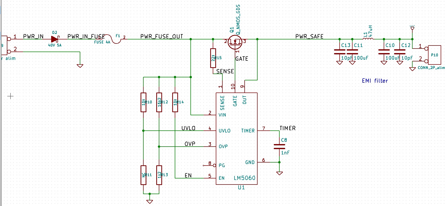
When I test it with a lab power supply, I start around 12V and gently ramp up to find the threshold.

It works perfectly and cut the power above 29V.

Now when I set the power supply to 35V or higher, and plug the cable, the LM5060 smokes, even with no load

We need a protection against 48V when our customers don't read the manual and plug our device to an active POE instead of 24V passive POE.

What is wrong with this schematic?

  • Vincent,

    You need to know the FET capability, specifically its SOA handling + Ciss, Crss.  You say the LM5060 smoked, was that the only device damaged or was there other damage? I suspect the FET may have burned, possibly because it cannot handle the turn on power dissipation.  The FET will see exactly the same energy that the output capacitor charges to.  1/2 CV^2 during the short power up time and a robust SOA FET is needed.  Look over the FET DS for input capacitance (for timer needs) and its SOA handling.  Measure input current (not output as the output caps may be between the point of measurement (current probe) and the FET.  You want to know what is passing through the FET along with Vin, Vout, Vgate, and timer pin in as many scope shots a you need to accomplish.  Given a 115mohm FET, it is a small die and may not be able to handle the total energy.  Total Cout is necessary, even any Cout off the schematic (not shown) to know the full conditions.  Try using the design calculator spreadsheet located at www.ti.com/hotswap to assist. 

    Brian 

  • Brian,

    First, thanks for your help on such a short delay.
    The transistor I use is STD10NF10T4 from ST (13A/100V/115mohm).
    It worked great after I replaced the LM5060. At power up, my load is under 0.25A/24V.
    For Cout, I have a CLC filter with 100uF/47uH/100uF, a DC/DC converter is directly after this.
    I don't have current probe.
    From what I understand with the design calculator, my capacitor on the timer pin is too small, I should have a 10nF instead of 1nF.
    Is Cgate mandatory?

    Vincent
  •  Vincent,

    Yes, the timer cap needs to increase, perhaps 10nF as you calculated.  What I suspect is that input inrush current into the 250uF Cout (~ 1ms rise time) is high (>10A) so the LM5060 is in fault condition at power up.  You can look at Vin, Vgate, Vout, and timer to see what is happening.  Observe the rate of rise on timer cap to know if it is 6uA (normal start up, dropping after Vgs reaches 5v) or 11uA (fault) charge current.  Do you have OVP still at 29v with 35v is applied?  UVLO is set ultra low, so Vin POR will turn on the LM5060 at ~ 5v.  If Vin is still rising, a inrush current will rise with Vin dv/dt (if slow) since the device turns on at such a low voltage.  Either way, if OVP trips, 80mA pull down on the gate will cause Vin at the LM5060 to rise to a very high level (exceeding DS 75v rating) and Vout to drop below gnd (rating -0.3v), either of which will damage the LM5060.  Likewise if the fault timout happens, 80mA will pull gate down and the same transient on Vin and Vout will occur.   See attahced di/dt impact pdf.  You will need an input TVS and an output Schottky (both high power) to suppress these transients.  The Vin transient is likely killing the LM5060.  The attached TVS and Schottky are very large ones to try, and you can back off from there based on your testing.  You can most likely drop to smaller versions but pick one of these to get info from in actual tests and you can also have SMB sizes handy after you get somewhere. You should borrow a Current probe at some point as you will want to know the current being dumped into the TVS.

    An RC for gate will lower the inrush current (slows Vout dv/dt) but you will need to make sure that total time for the normal 6uA start up charge into Ct is long enough for Vgate to rise to 5v per the DS and also that you are below the fault level where the 11uA current kicks in.  Longer Ct will increase the time the device sees an over load current so watch that.  For the Gate, use a 1k in series with an added Cgate.  The resistor isolates the Cgate so the 80mA effectively pulls down the FET gate.  

    Brian

    Voltage transient protection for HS due to di_dt CB event.pdfOutput Schottky SK153.pdfLittelfuse_TVS_Diode_5_0SMDJ_Datasheet.pdf