This thread has been locked.

If you have a related question, please click the "Ask a related question" button in the top right corner. The newly created question will be automatically linked to this question.

TPS7A33: Output noise increase over time.

Part Number: TPS7A33
Other Parts Discussed in Thread: TPS7A47

Using TPS7A family to provide regulated low-noise symmetrical (+/-24VDC) outputs per schematic fragment below:

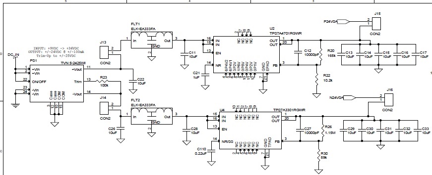
TPS7A4701 and 3301 are set for +/-24VDC output (per data sheet), LDO input from Traco TVN 5-2425, trimmed up to +/-25Vdc.  LDO input signal noise + ripple:  < 2mVpp.

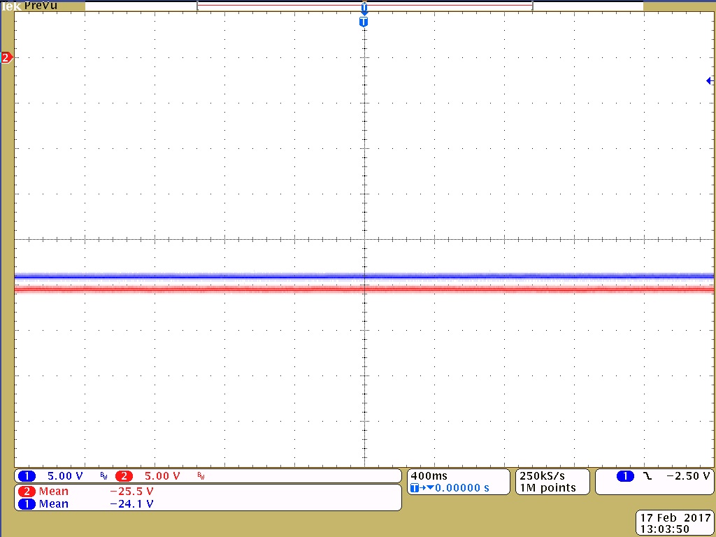
No load, open circuit scope measurements.

When PCB is powered up -> day #1 -> LDO signals measured @ J15/J16 pin 1: TOP trace - BLUE: -24VDC output,  AC coupled., Bottom Trace: RED +24VDC output, AC coupled.  Low noise on both rails.

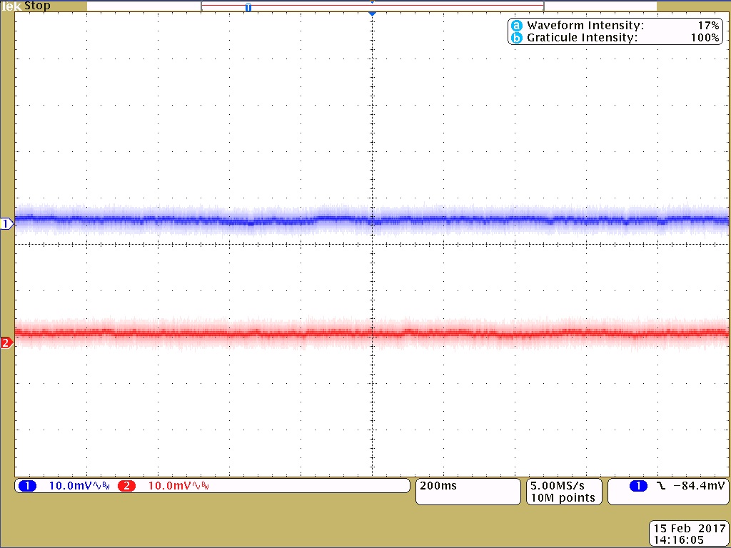
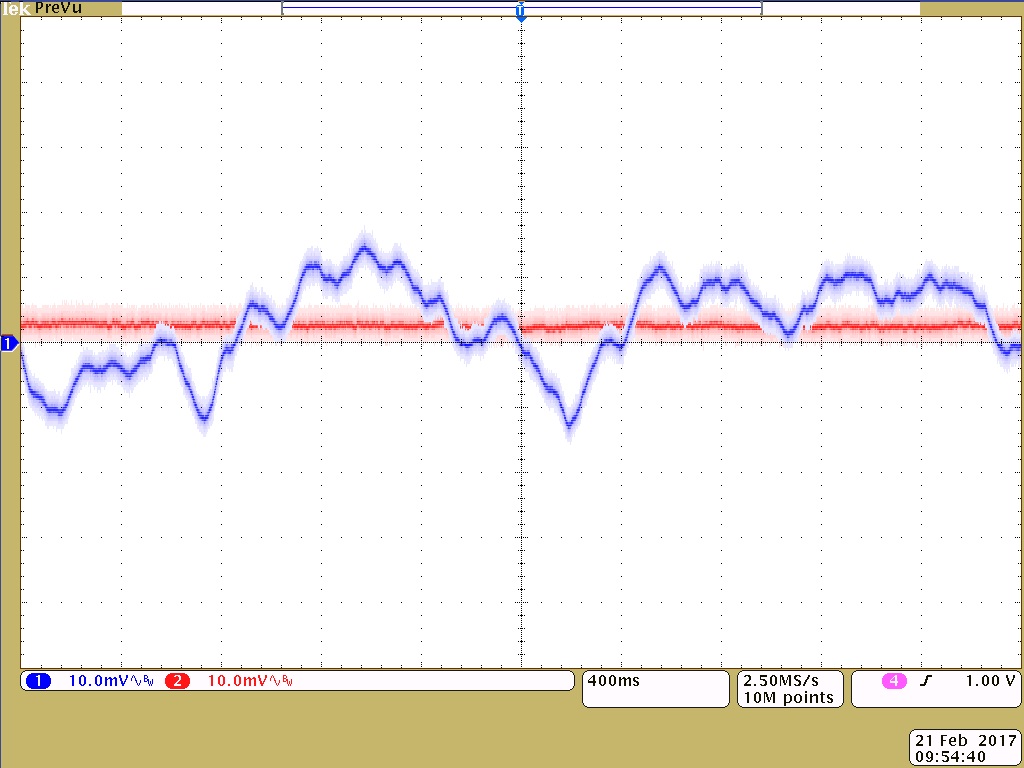
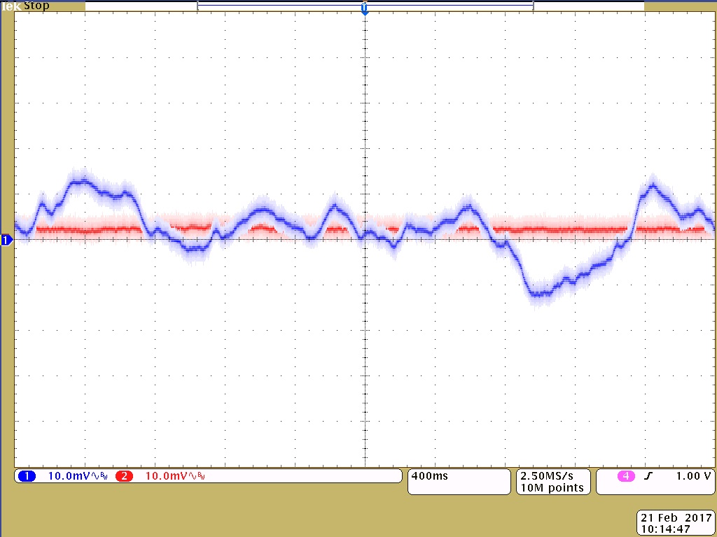
PCB left running in LAB overnight:  Noticeably higher noise on -24VDC LDO output.  Power recycled.  No change.  Repeated on three (3) identical prototypes.  Identical results.

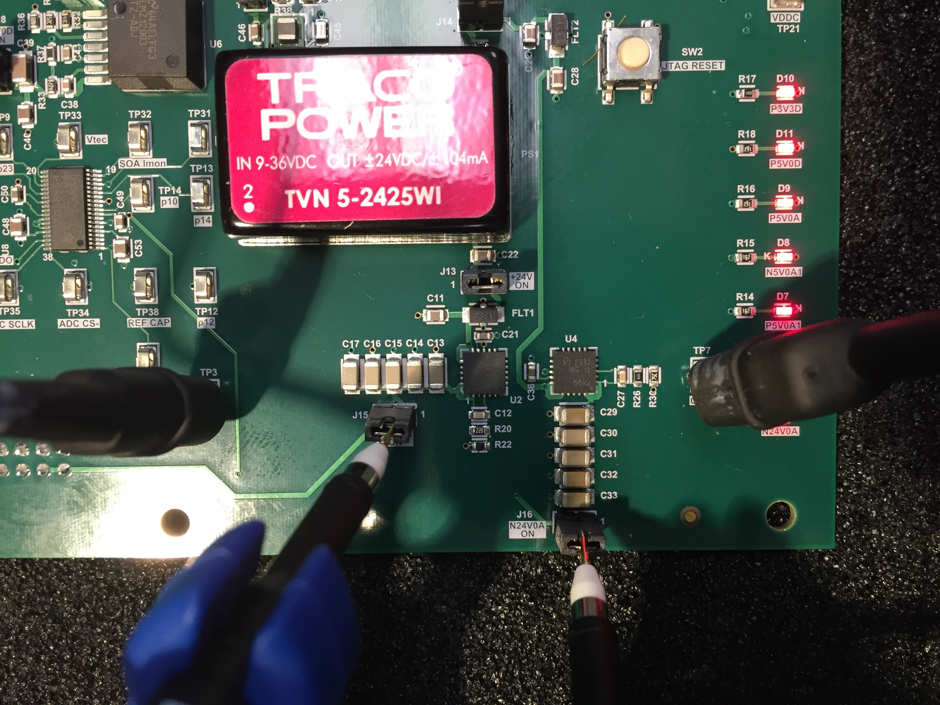
PCB Layout shown below, top side assembly and Layer 1 routing.  Ground plane on Layer 2.

Any help would be greatly appreciated.

  • Hi Joel,

    In order to help debug, could you also provide DC coupled scope shots of the inputs and the outputs? Furthermore, could you provide scopes shots with a load?

    A couple comments about your layout snip: 1) The prefilter and input capacitor for your positive rail are close to the TPS7A47, while your prefilter and input capacitor for your negative rail are further away (enough that they do not show on the partial layout you provided). Placing a localized capacitor at the input pins of the LDO will improve AC performance.

    2) We recommend having a ground path on the same layer of the PCB as the LDO. Having the capacitor grounds going through vias increases the ESR and ESL for the capacitors.

    Very Respectfully,
    Ryan
  • Ryan:

    Will do.

    Per suggestion #1.  I had our technician solder a 10uF, cer cap, X7R, 0805, at the chip.  No change in output ripple + noise.

    I will send the requested data shortly.

    Thanks,

    Joel M.

  • Ryan:

    Scope traces:  NO LOAD - LDO Input and output - DC coupled - RED trace = LDO input V, BLUE trace = LDO ouput V.

    Scope traces:  -17mA LOAD - LDO Input and output - DC coupled - RED trace = LDO input V, BLUE trace = LDO ouput V.

  • Hi Joel,

    Thank you for the additional information. Could you provide the last scope shot (with load) AC coupled as well?

    Very Respectfully,
    Ryan
  • Ryan:

    Per your request.

    A PIC of the PCB showing my measurement setup (scope probes and GND clips)

    RED TRACE = +24VDC, AC coupled, NO LOAD

    BLUE TRACE = -24VDC, AC coupled, NO LOAD

    RED TRACE = +24VDC, AC coupled, 37mA load

    BLUE TRACE = -24VDC, AC coupled, -37mA load

    Thanks,

    Joel Mock - MOI

  • Hi Joel,

    There are only a couple of things that I can see from your schematic/layout that could be done to improve your noise performance on the negative rail. Schematic wise, the NR cap could be increased which would filter band gap noise internal to the LDO. Layout wise the long input trace running right next to the switcher and lack of ground on the top layer allow for noise to couple to the input of the LDO.

    Very Respectfully,
    Ryan