


Hi
1. Based on the input we received for the thread "UCD9090 Power Down sequence Implementation Issues" from TI Forum, we implemented the system reset functionality and used this to toggle the control pin state.
System reset is decided by the power good of 5V (board main power input coming from external supply) and the tracking state of GPI (GPIO16). When the GPI goes high, control pin goes low and makes the power cycle. The GPI is driven from a CPLD (powered by the 3.3V) when we need a complete board power cycle(off course except 5V). We need to validate this implementation. I have attached the schematic snap shot and the project file.
2. We are seeing a power glitch on all the GPO lines at the same instant when the board power gets in, which we haven't faced in our Proto1 design.Since the glitch is going till 1V, two regulators (we are using TLV62084DSG for 1.8V & 2.5V) turned on when the board power comes in. This is because the regulator has an EN threshold around 1V.
We are doubting that the Loop formed due to the system reset.
Kindly review the schematic snap shot and the project file and give your input.
Regards,
Felix.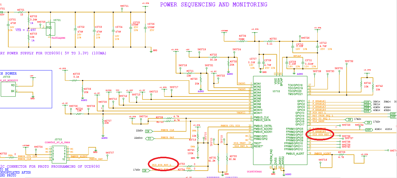 g430v3_u3702_v2.xml


