This thread has been locked.

If you have a related question, please click the "Ask a related question" button in the top right corner. The newly created question will be automatically linked to this question.

LM25085: LM25085 Buck converter not working when loaded

Part Number: LM25085

Support Path:/Product/Development and troubleshooting/Search the forums for my problem/

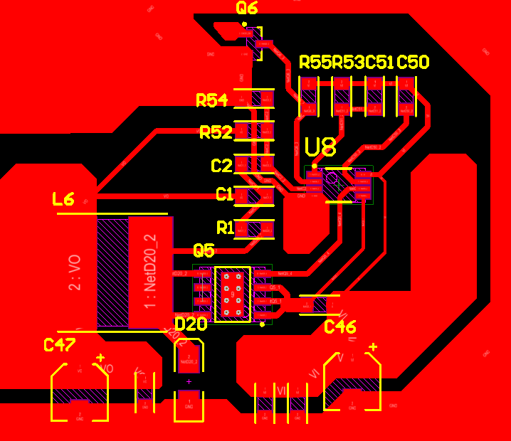
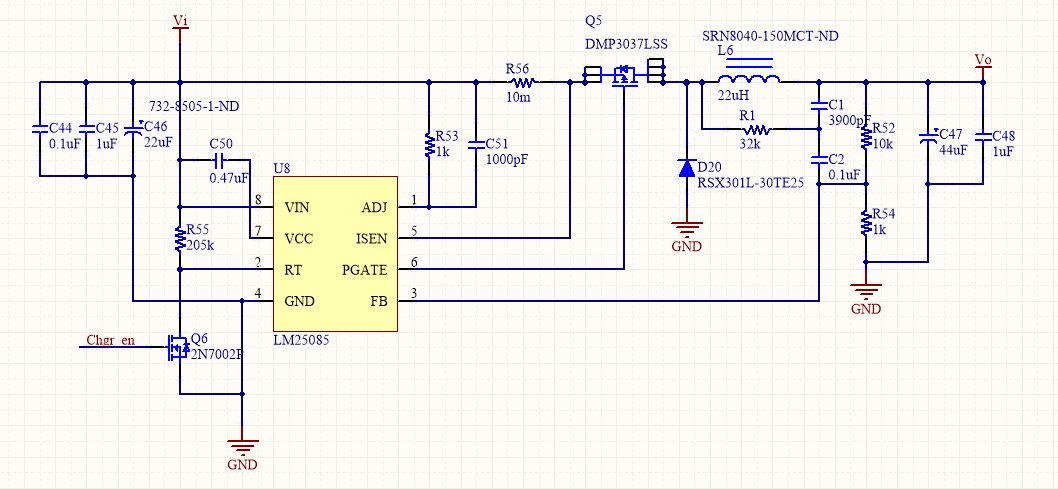
Hi, I'm trying to build a lead acid battery charger using the LM25085 but having some trouble. Input to the converter is 18V and the desired output is 13.8V. To test the circuit i have made a single layer board and added the schematic and layout below. the schematic includes the part numbers for the mosfet, diode, inductor and input capacitor. The output capacitor is simply 2 of the input capacitors in parallel

The converter works when it is not loaded and i measure 13.8V on the output and 1.25V on the feedback pin. However when i place a 22ohm power resistor at the output the converter fails and the output voltage drops to a very "noisy" 1.3V and provides 0.06A.

I suspected the issue is from the ripple generating network but trying different values (1uF, 0.1uF, 4nF 0.033uF) for C2 did not have any effect.

Im able to provide other information including oscilloscope captures. At this point i'm not sure how to debug the circuit, any help is appreciated.

  • According to my calculations R1 should be around 60k, but I don’t think the value you have is the issue. Perhaps you are hitting ILIM early due to noise on the current sense input? You may want to try a 100ohm in series with the line going back to Pin 5 (ISEN) of the IC? Also place a filter cap from Pin 5 to pin 8.

    Looking at your layout, it does not look ideal to me as all and could well be related to your issue. You need a ceramic very close to the Top FET Vin connection (Or Rsense in your case) and the Anode of the Diode. This loop needs to be minimized (kept small). Section 10.1 in the datasheet details how to layout the IC and power components, I strongly advise following the layout guideline therein. I also would take a look at the EVM and see example of the layout and suggest following this layout pattern.
  • I changed R1 to 60k and as you suggested I tried placing a 100ohm in series to the with pin 5 and a 0.1uF ceramic across pin 5 and 8 but the problem still exists. You also mentioned placing a ceramic from Rsense to anode of the diode, however there's already a 0.1uF and 1uF(C44 and C45) they are next to C46 in the layout and not labelled. Regarding the layout since i can only test on a single layer board this is the best I can do.
    Doing some more testing I realized that the converter keeps regulation at very light load (upto 0.1A) and fails if load is increased any more. Probing the SW node shows that it never drops to 0.4V (Vf of the diode) as expected and tracks the output voltage so i suspected that the diode can be the issue. The circuit behaves exactly the same with or without the diode soldered on.
    Another observation was that earlier I had a 22uH inductor on the board and nothing worked, changing the inductor to 15uH helped with that.
  • Hello,


    the filter cap I was referring to was a capacitor connected to the 100ohms in series with ISEN(pin 5) and Vin.  use a 100pF and increase to 1nF if needed?  See if tis helps?  Also please can you take a scope shot of the converter working?  Please can you take a scope shot of the Switch node at light loads?  Thanks.