Hi,
the switch node voltage can exceed max ratings in certain conditions. I would like to know if these issues has to be taken care of?
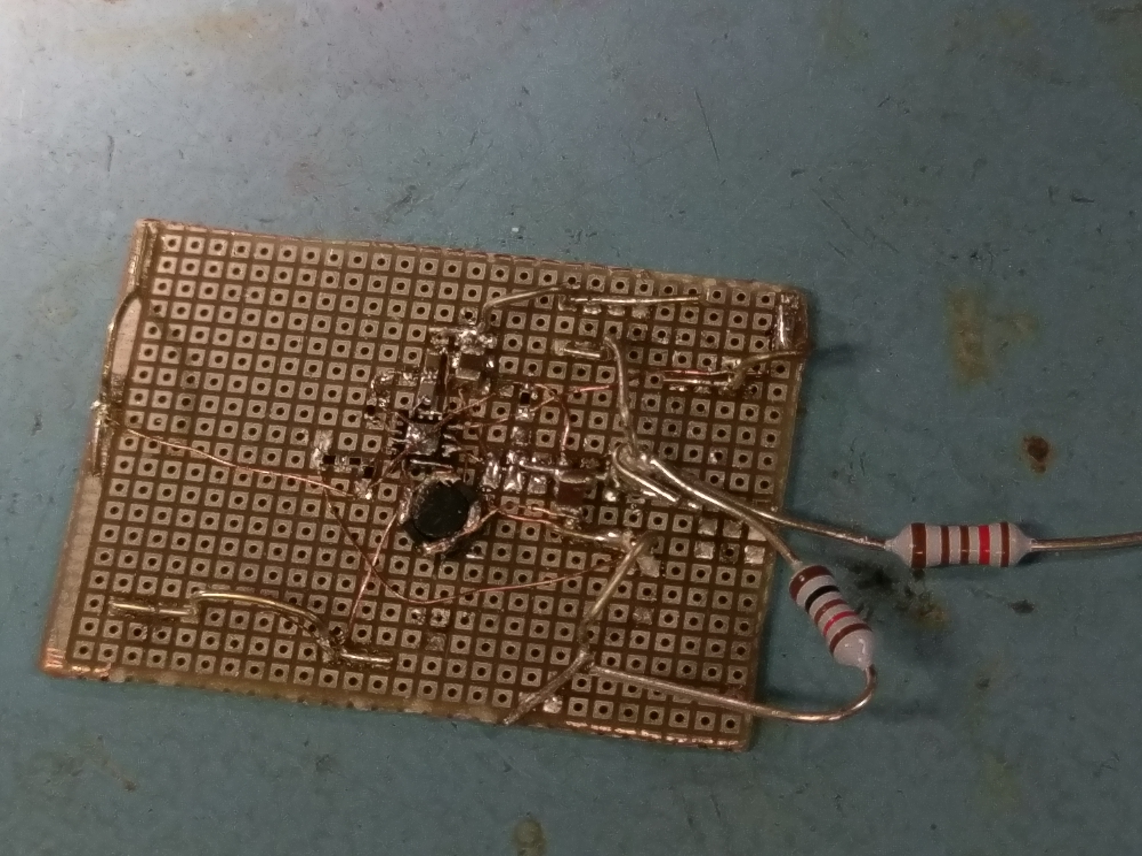
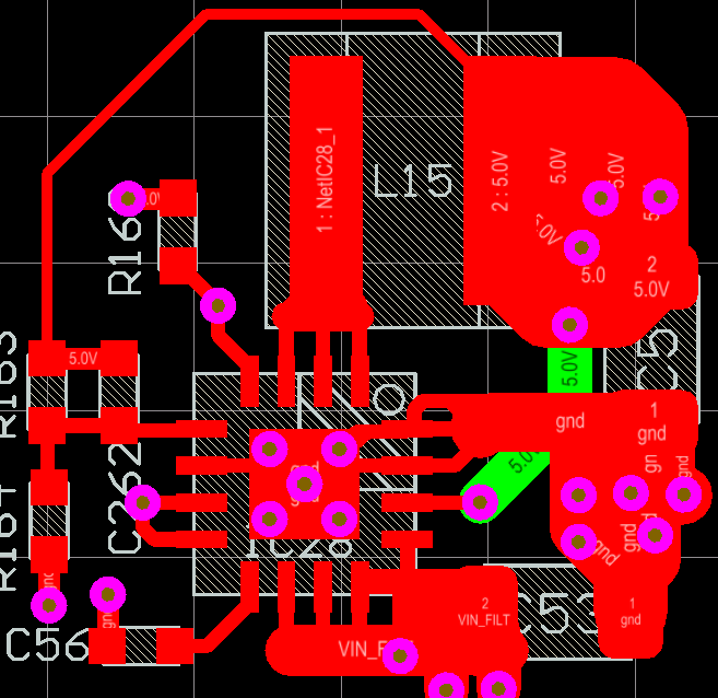
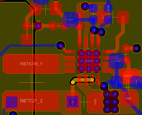
I've attached two pics from two designs: 5 to 3.3V (on a simple breadboard), and 8 to 5V (from a PCBA with layout as shown in the data sheet).
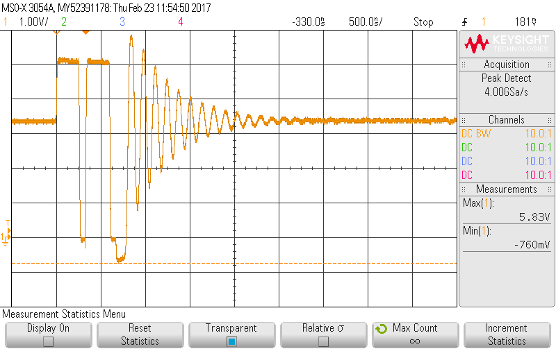
1) The minimum switch node voltage rating of -0.3V is exceeded due to the inductor current through the internal pass diode when the synchronous rectifier is turned off. The first picture (5 to 3.3V design) indicates a min voltage of -0.76V. it might be slightly better on a real PCBA.However, the second picture is from a PCBA, and there's still -0.7V undershoot. Is this acceptable?
2) Max ratings on switch node is Vin + 0.3V. As seen it can easily be exceeded due to the ringing at the node during discontinous mode. Do I need to add an RC damping to the switch node to reduce the peak voltage?
I always pay respect to the Max ratings, but I also would like to trust the designer of the device being aware of the actual behaviour of the design, so I'd like to think that the min voltage rating of the switch node actually is "better" than -0.3V. The max voltage rating I fear is more absolute?
BR
Picture 1: 5 to 3.3V on breadboard
Picture 2: 8 to 5.0V on PCBA