This thread has been locked.

If you have a related question, please click the "Ask a related question" button in the top right corner. The newly created question will be automatically linked to this question.

TPS54540: TPS54540 HF noise

Part Number: TPS54540
Other Parts Discussed in Thread: LM2677, LM25085A

Hello,

I have design a power supply 29V AC input to 24V 5A output.

I have use the TI webench for choice my component.

In the TI webench, it say 2.8mV of noise.

I have design my board in suiting the TI recommendation, i have see the TI documentation about noise "www.ti.com/lit/an/slyt682/slyt682.pdf"

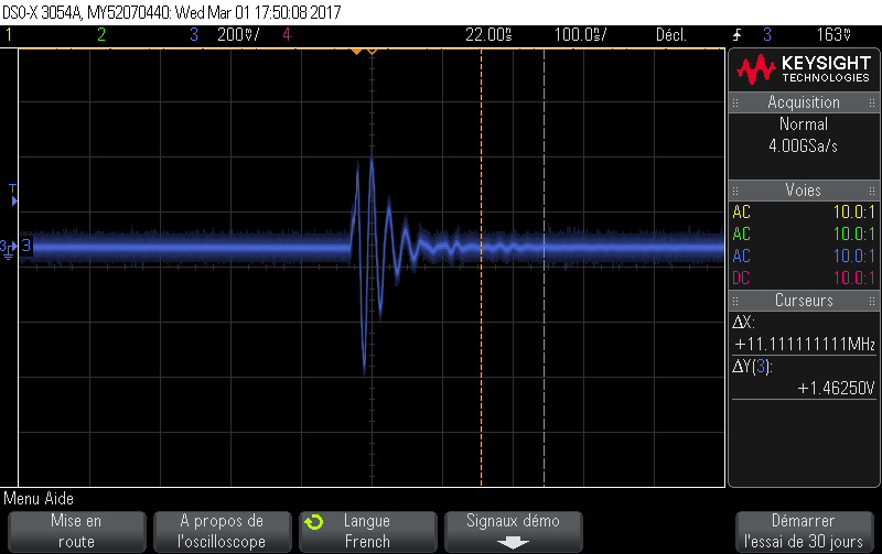
I have test my board, (0.7A and 1.5A) i have 190mV of noise HF, the frequency is 50Mhz. The noise appear when the SW pin change.

The switching frequency is 129Khz, the output capacitor is low ESR

My schematic:

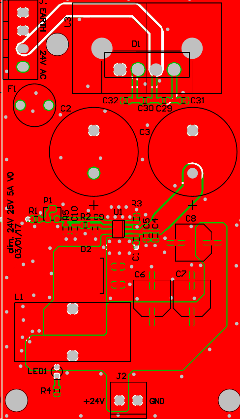
My PCB: the board have 2 layer and copper thickness is 70µm.

The oscillo picture:

HF noise

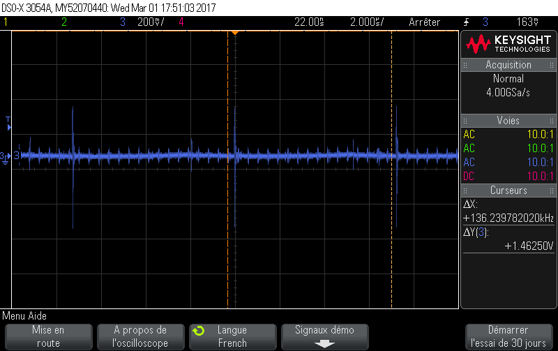
Decoupling frequency:

I have test to change self, to shielded self, no amelioration.

I have change the STPS20M100S diode to other diode (TPS5100-13) but the noise is increase.

Do you have solution for reduce HF noise?

Thanks

  • I do  not support TPS54540 directly but I do have some familiarity with it.  The first thing you should note is that you have to be careful when measuring the switching noise.  It is best measure directly across the output capacitors(s) using a very short ground lead (<1cm) or better yet, "tip and barrel" method.  That said some of your switching noise is probably real.  Isee you only have electrolytic capacitors on the output.  They will not be effective in reducing high frequency noise, especially if you are measuring at the J2 output connector.  The output capacitors and output connector are not well placed relative to each other.  You will want to add some HF decoupling on your output. 1uF, 0.1uF and 0.01uF probably close to J2.  I would rearrange the output so the connector comes after the output capacitors for maximum effectiveness.  You may also want to consider an RC snubber from the SW node to GND.  Included is a document to help you design it.

    5265.RC Snubber.pdf

  • Hello,
    Thanks for reply.
    I have test the RC snubber.
    If i add capacitor between SW and Vin pin (parallel to the hight side mosfet), the frequency dont change, but if I set more capacitif (100nF) the output voltage decrease (8V instead of 24V).
    I have the same result between SW and GND.
    The only solution i have found for reduce the noise is to add a Ferrite in serial to the output and add large capacitor after (capacitor for remove low frequency noise).
    Thanks
  • A snubber from SW to GND should help. Did you follow the instructions closely?
  • Yes, i have test a lot of capacitor in increased value from 20pF to 100nF, but i don't have find the frequency divided by2.
    I have solder capacitor directly to the pin of tps54540.
    I don't have add a resistor.
    Thanks
  • Hello
    I have other problem:
    If i start the TPS at no load or little load, i have the 24V dc at output
    But if i start at full load the TPS can't start, i have 2Vdc in output
    If I start at no load, wait the output rise to 24Vdc and put up the full load, the TPS output is ok and the dc output is stable at 24Vdc
    I have test in adding 2 resistors diviser in EN pin, (between Vin and EN , EN and GND) but same result.
    Do you have idea
    Thanks
  • It is possible you are running into current limit at start up. How much output capacitance do you have?
  • I test the power-supply with a power resistor, about 9.2 Ohms for have 2.6A.
    I have measure the current (current probe with oscilloscope) in power resistor, i don't have a big peak in start-up, it not exceed 2.8A.

    Thanks
  • I have find the solution, but i dont have the explanation:
    I have change my diode (STPS8H100) 8A 100V to STPS20M100S 20A 100V, the TPS54540 start even in charge.
    But i don't understand what is the problem of STPS8H100.
    Thanks
  • TPS54540 is in fact sensitive to diode selection.  It could also be an issue with your layout.  Adding an RC snubber from SW to GND is also known to improve this.

  • Hello, I found other documentation of TPS54540 and noise suppression www.ti.com.cn/.../slvu973.pdf
    In this documentation, they add snubber in SW pin.
    In my precedent post, i haven't measures the noise in SW pin but in output after the inductor.
    I had restart the measure in SW pin and i found the RC value.
    In other side, i have test my board with 5A resistive, but the output voltage is saturated to 10V, and if i see in SW pin, i am in DCM mode.
    I have increase the frequency, the output voltage are increase to 17V, but the output voltage in not stable (25ms at 17V and decrease to 0 like a capacitor discharge and increase to 17V like a capacitor charge.
    I have decrease my inductor(15uH to 5.5uH) the output voltage have increase to 20V, but as previous, output is also not stable, but the periode is 100ms.
    I can't more decrease my inductor because it increase the output current of TPS and i'm near to limit (7.5A).
    I'am not sure that TPS54540 can supply 5A with 24V in same time.

    Do you have other TI buck converter (prefer integrated MOSFET) who can provide 24V and 5A certified by TI (existing evaluation Module for exemple)
    Thanks
  • I have tested a LM2677, same result:

    It doesn't have 24V and 5A at the same time in output.
    My supposition TI doesn't have any switching regulator which have integrated MOSFET who can have more than 15V and 5A in output.

    My next step is to test a LM25085A, which has external MOSFET.

    Thanks