A related question is a question created from another question. When the related question is created, it will be automatically linked to the original question.
If you have a related question, please click the "Ask a related question" button in the top right corner. The newly created question will be automatically linked to this question.
Hi ! I'm using the UCC2895 and got some problems.When IC power on, I can't get 5V in 4(ref) footprint and sawtooth wave in 7(CT)footprint.It means the IC is not work and the Power is ok.
Would you share your schematic to let me know how did you configurate the IC and what is the voltage at VDD pin? Please notice that VDD should great than UVLO thershold(11V) to get the IC work.
Hi Oliver,
Firstly,Thank you for your help!I study some documents about UCC3895.There is a transistor between REF(4 footprint) and RAMP(3footprint),its purpose is to realize the downslope compensate in peak current control.Can I directly connect the CT(7 footprint) to the RAMP(3 footprint)? If it is ok, the capcitor between RAMP footprint and GND is useless,can I take if off?
To minimize loading on the oscillator, it is best to buffer the timing capacitor(CT) waveform with a small transistor between REF and RAMP. The small capacitor between RAMP and GND works with a resistor as a filter to bypass the noise from current sense.
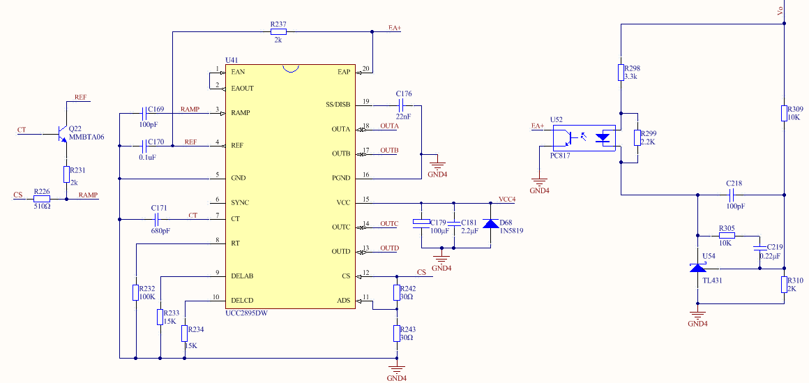
I'm really appreciate for your help! I study the datasheet and user's guide again,and get some questions.
1. The output of the small transistor connect a resistor to the RAMP, how to design the value of this resistor?
2. Assume the VBE=0.7V, it means that only the voltage of sawtooth above the 0.7V, the RAMP footprint can get the voltage. This will result in the duty ratio jump in smaller duty cycle, is there any methods to solve this problems?
3.The ADS and CS footprint has a resistor respectively, how to confirm the value level?
4.This is my control schematic, please help me check it out.
The calculation of slope compensation components is suggested on page 3-106 and 3-107 of U-111, the app-note describes the whole details better than I can. For the ADS configuration, please use equation 5&6 in the datasheet to determine the resistors divider. The resistor value should as large as possible to avoid sourcing too much current from CS but need to provide enough bias current(+-20µA) for this pin.