This thread has been locked.

If you have a related question, please click the "Ask a related question" button in the top right corner. The newly created question will be automatically linked to this question.

BQ76200: Reg Issue in High Switching Frequency

Part Number: BQ76200

Dear All,

we are using BQ76200 in our design and We have a problem with high si 
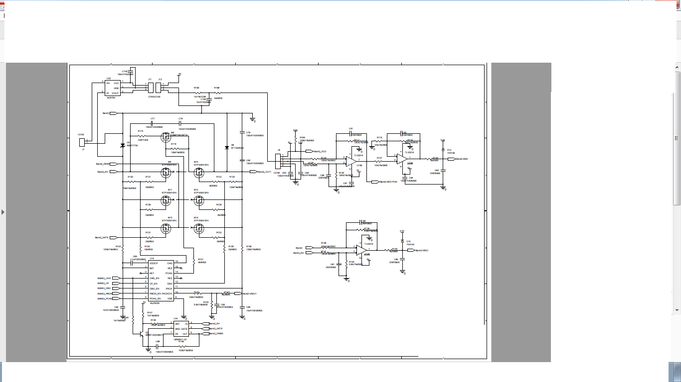
de driver BQ76200 in high switching frequency (more than 100Hz)

I have attached schematics of BQ76200. Kindly review and give solution.

Non Populated Components:

R146,R147, R148,R149,C96,Q2,U16

M13,M14,R115,R116,M8

Value Changes:

C89 = 2.2uF (2 in parallel)

NOTE: All the MOSFET Drain Connected electrically through a Heat Sink.

Rgds,

Aravind.

  • Hi Aravind,

    Unfortunately I can't read the component values or net names on the schematic.

    See the application note bq76200 Beyond the Simple Application Schematic. Common causes of a failure to turn-on with switching at 10's or 100's of Hz such as figure 5 are:

    • A small charge pump capacitor, but your note looks like you have increased this.
    • Too large of a PACK pin filter capacitor. 10 nF is typical
    • Too small of resistors from the FET gate to source.  10M is typical.
    • Too much switching loss when turning on DSG.  A few hundred ohms between DSG and the gates can reduce current into the PACK pin capacitor, a zener and resistor between the DSG and PACK pins can reduce internal losses. 

    Switching CHG_EN and DSG_EN at separate times can help turn on or reduce the size of the CVDDCP capacitor.

    If I have misunderstood or if you can post a clearer schematic, please let us know.

  • Hi Aravind, the link for the apnote originally posed above did not work, it is now corrected.
  • Dear Sir,
    Customer made changes and tried to increase the Switching frequency but still not able run more than a 50Hz, please advise suggestions.

    Aravind.
  • 6136.SCHEMATIC1 _ PAGE4.pdfDear Sir,

    I have also attached clear schematics for your kind reference, please check and help to provide valuable suggestions.

    Aravind.

  • Hi Aravind,

    I misunderstood.  The customer has a datasheet-like schematic.

    The part builds charge in the charge pump capacitor, their C89. When switching on the FETs, some of this charge will move to the FET gate capacitance.  The current flow in the internal resistances will have some switching loss as power.  With DSG there is the possibility of loss into the internal zener paths and the PACK capacitor as shown in the application note figure 10. After turn on the charge pump will build up the charge pump voltage again to normal. When switching off the FETs, the gate charge is dumped to GND (DSG) or BAT (CHG), it is not available to the charge pump again.

    When switching repeatedly, once the charge into the FET gates and switching loss exceeds the charge pump capability, the charge pump voltage will drop enough that it will cycle the drivers.  I don't know an equation for how fast it could switch.  The part is intended as a battery protection switch application where switching is slow.  Reducing or removing the PACK pin capacitor would allow the fastest switching since the PACK pin would not be held down by the capacitor, although the net capacitance will not be 0.  If the FET came up fast enough losses in the zener paths will be avoided.  Reducing the FET gate capacitance  would be the other way to switch faster. 

    The internal power losses from switching can't be eliminated.  Removing the PACK capacitor (C95) will expose the pin to transisnts on Bank2_OUT+, so it should have transient protection.  Keeping R136 will help isolate the pin.  Having non-zero R134, R135, R137 will reduce transients coupled through the FETs but increase switching losses. 

    A larger charge pump capacitor likely won't help here since the issue is apparently the current capablity of the charge pump.