This thread has been locked.

If you have a related question, please click the "Ask a related question" button in the top right corner. The newly created question will be automatically linked to this question.

Apparent TPS 40200 design mistake. HELP

Other Parts Discussed in Thread: TPS40200

Hello Specialists..

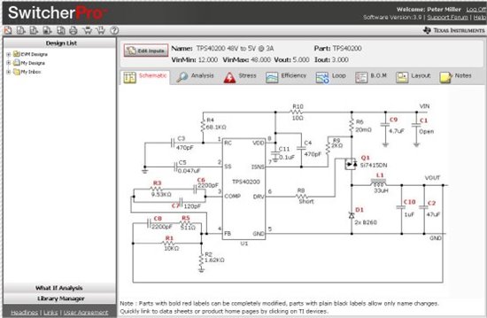
I've designed a switching power supply using the TPS40200 controller. I made it using the SwitcherPro tool offered in TI Website.

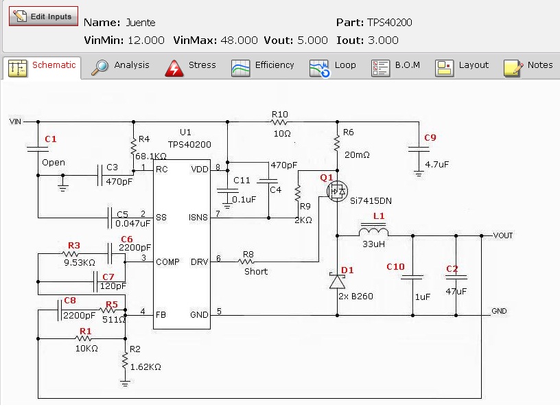
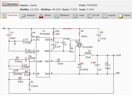
If you try a design with the followings parameters,

TPS40200

V input min: 12V

V input max: 48V

V output: 5V

I output max: 3A 

you will see a resistor (R10) of 10ohms between Vcc INPUT and the (C9) 4.7uF pump capacitor. Such resistor is a 0805 standard which does not disipate more than 0.10W. I think there is a mistake in the VccINPUT point of entrance. Shouldn't it enter from the 4.7uF end? That way, R10 will serve as Low Pass filter altogether with (C11) at the TPS40200 Vdd input (pin 8).

If I connect Vcc INPUT in the point specified in the SwitcherPro schematic, (R10) will not supply enough current to the 4.7uF and MOSFET.

Another question is: There is NO consistency between Schematic and Layout presented in the same SwitcherPro tool. You will find there is no resistor between Vcc INPUT and Rsense. Moreover, Rsense is (R6) in the schematic but this appears in the place of (R2), the FeedBack for the TPS40200.

I think there are some mistakes with SwitcherPro, let me know if I am wrong. And let me know too whether proceed with ensambling or not.

Tahnk You very MUCH.

Eng Ivan Perino

UNSL, Argentina


  • Yes, R10 should be in a vertical orientation between VIN and VDD, forming a low-pass filter with C11.


    When R10 is used, the time constant R10 * C11 should be equal to the time constant R9 * C4


    I will look into the layout / schematic reference designator issues.

  • Peter, I note that Switcher PRO still produces this erroneous output. This should be highlighted and fixed.

    Regards,


    Dale Gomes

  • Dale,


    Thank you.  We are aware of the issue and it is scheduled to be fixed.  I am not sure if it can be accomplished as a hot-fix or if it needs to be incorperated as part of a revision release.  I will check.

  • I too have just realized this error in Switcher Pro today. Unfortunately after the 20 PCBs have already been made.  :(

  • Peter,

    Has this error been fixed in the latest SwitcherPro release? If not, can you please clarify what you mean by "R10 should be in a vertical orientation between VIN and VDD"? I am having a problem with a circuit using the TPS40200 as it is recommended in the SwitcherPro schematic.

    In the picture shown in the first post, when you say "R10 should be in a vertical orientation" do you mean that R10 should be connected in parallel with both R4 and R6, rather than in series with R6 as it is shown?

    Thank you,

    -Kim

  • Kim,


    I've checked the on-line version of SwitcherPro today:

    The switcher pro team decided to move VIN and C1 from the right side of the circuit to the left side of the circuit to correct the configuration.

    If you have the desktop version of Switcher Pro, you will need to update your version for this change to take effect.

    The critical factor is:

    R10 should be between the power stage input voltage (VIN) and the VDD pin of the TPS40200 controller (Pin 8).

    In the original schematic VDD was directly connected to VIN and R10 was located between VIN and R6, which required all of the power stage current to flow through R10.

  • Kimberly,


    For clarity here is the original Switcher Pro schematic with the change I was trying to describe in RED


    R10 has been moved into the vertical trace between the VIN node (the node across the top of the schematic with connections to C1, R4, R10, R6 and C9) and the VDD node with connections to U1 Pin 8, C11 and C4.

    The above schematic and the new switcher pro schematic (from my last post) are slightly different electrically.  In the above schematic R4 is connected from VIN to RC (U1 Pin 1) while in the new switcher pro schematic R4 is from the VDD node (U1 Pin 8) to the RC node (U1 Pin 1).  The new switcher pro schematic is actually the prefered configuration as this draws the oscillator current (current through R4 into RC) and the oscillator peak-voltage reference (VDD / 10) from the same voltage and improves the voltage feed forward functionality during a line transient.

    Again, I apologize for any issues or errors this graphical mistake in Switcher Pro has caused.