This thread has been locked.

If you have a related question, please click the "Ask a related question" button in the top right corner. The newly created question will be automatically linked to this question.

TPS40200: Inverting supply: IC draws excess current while switching, gets hot

Part Number: TPS40200

The design in question is an inverting -13V supply from 28-36V input (VDD="VSUP2").  The exact same design/layout/values/etc works fine in non-inverting +13V form, but when the inverting switcher turns on (begins switching), the TPS40200 IC begins drawing approx. 0.013 A @ 20 Vin. 

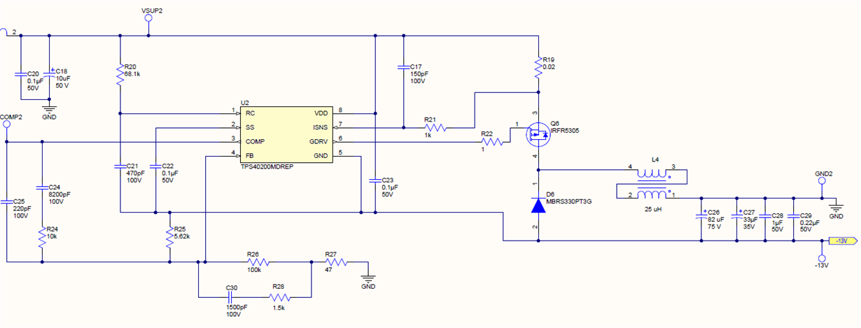
NOTE:  1) C18 and C20 actually connected from VDD to -13V output.  2) Inductor L4 value is actually 100 uH

TWO QUESTIONS:

1) What do you think might be causing the IC to draw excess current?

2) Also, the only way I can get the supply to start (overcome OC conditions, upon startup) is to briefly jumper TPS40200 pins 7,8.  After startup, the jumper can be removed and the circuit continues to operate.  Do I need to increase the values of R21 and C17 in the ISNS network?

  • Trying to post a copy of the schematic, but will not post after it is pasted into the text box...
  • Schematic posted...
  • Let me see if I can find someone to answer this.
  • Issue #2 resolved/fixed after increasing value of C17 to 0.1 uF.

  • Hello,

    If you have a 1k series resistor, the 0.1uF, is very large. Make sure that the design works reliably under all short circuit conditions. it is likely layout and the way the sense lines feedback to the IC that is causing the issue. You may want to reduce R19 rather than increasing the time constant of the RC current sense filter? regarding your current measurement, are you measuring the input current to the converter, or specifically measuring the input current to the IC? Please can you confirm? Thanks.
  • I am measuring input current to the converter (entire circuit) from the power supply, however, the thermal camera shows a 30-40 degrees Celsius rise within U2 (TPS40200 IC) package.  Exact same circuit layout, components, etc in non-inverting +13V supply draws only 4-5 mA @ 20V, while switching, and TPS40200 temperature rise is only 5-10 degrees Celsius higher than ambient temperature (approx. 25 deg C in the lab).  Tried replacing transformer, then tried isolated flyback transformer (completely decoupled switching node from output node), then built a 2nd prototype with only components shown in schematic -- all with same results (TPS40200 circuit draws 16-18 mA @ 20V in inverting configuration, with U2 the "hot spot" 30-40 deg C temperature rise above ambient)

  • The temperature will increase on the board in general. the light load, no load efficiency will always be worse in an inverting configuration. Therefore the input current will be higher because the inverting supply can be viewed as Vin+Vout (modulas) for the Vin and Vout is always 13V. Put another way, the Vin max of the convertor is 13V+36V = 49V in. Now with this higher Vin, the transitional losses and switching losses as well as the core losses will be worse in the inverting configuration, this is not load dependent. Therefore the input current will certainly increase. Secondly, the IC temperature will go up, because the Gate Drive currents (Qg x Fsw) is being supplied from a higher input voltage (referenced to the Gnd of the IC which is a differental of 49V), that the parts sees, and with the Vin to Vout differential being greater, the losses on the IC will be higher as a result.
    I believe, If you measure the input current on the VDD pin with of the IC with a DVM and multiply this by 36V for the non inv case and then multiply with 49V for the inverting case, it will be apperent why the losses are higher?
  • Agreed, efficiency of inverting config will be worse than non-inverting, and higher Vin will result in higher switching losses.  However, the non-inverting (+13V) supply current only rises 1-2 mA when Vin is increased from 20V to 40V.  With respect to the inverting (-13V) config with Vin = (20V - (-13V)) = 33V, the supply current is 300% greater than non-inverting.  This is an embedded design intended to run on battery power (28-36 V), and ~50 mA light load (on each of the voltage rails).  I am concerned that the light load efficiency is not good enough for the application but want to confirm that schematic is correct and that there isn't an adjustment that can be made to the circuit (layout, component selection, component value, etc) to improve the light load efficiency (prevent so much power from being dissipated across the TPS40200 in inverting config).  Any suggestions?

  • I rechecked your schematic and note that your Schottky Diode is a 30V VRRM device. With the conditions mentioned above, the diode will see 33V. Please can you replace with a 60V Schottly and retest, to satisfy the full range of your specification?
  • Changed MBRS330 to BAT46Wh (100V VRRM) and current draw remains unchanged. I suspect at 25 deg C, the MBRS330 had a bit of safety "guard band" built into the 30V VRRM, so it wasn't breaking down. Good catch, though. Thank you. Any idea why the TPS40200 is still getting hot?
  • Hmm,
    Can you take a scope shot of the switch node with the inverting supply running? I want to see if its stable? Also please take a scope shot of Vgate to the P Channel MOSFET. Thanks.
  • The P-ch MOSFET may be getting too much voltage on its G-S junction (most can only do 20V at most,) and possibly biasing any G-S diodes in it into conduction, which would ask for more drive power from the IC, increasing its losses. It may be necessary to level shift and/or amplitude shift the MOSFET gate drive with a transformer or other means.

    Also, setting up some switching means to limit the Vcc on the IC will reduce its dissipation further. This could mean switching its supply to the output after startup, an inductive auxiliary supply pickoff, or other method.
  • Hi Gordon,

    Not sure I follow you? The Voltage between the gate to source on the PCH MOSFET is regulated (VIN-8V?). It should not overdrive at all?
  • Sorry, I replied too quickly and didn't confirm the datasheet. My bad. Never mind about the G-S overvoltage part of my comment. Also the note about supplying the Vcc differently has to be rethought.

    But after a look at the datasheet, the Vcc-8V supply for the P-Ch MOSFET will dissipate much more in the -13V case than it will for the +13V case. It is the linear regulator inside the IC that is dissipating the power supplying the (vcc-8V) charge to the MOSFET gate and dropping 41V (assuming Vin-Vout=49V) inside the IC. This, being up to 300 mA PEAK current, (and average is likely >3 mA,) certainly accounts for some of the dissipation. To minimize this dissipation, the total gate charge has to be minimized; the Miller charge is considerably more than if trying to run as a +13V supply because the drain voltage swing is 49V in the -13V case but only about 20V in the +13V case.
  • Agreed,

    As mentioned the DC current is ~ Qg total x Fswitch. If you wish to minimize the losses due to the gate charge, you will need to select a MOSFET with a lower total Qg. If you select a low total Qg and the temp rise reduces, you know you are headed in the right direction. You may want to select a lower switching frequency too?
  • Looks like 300 kHz switching frequency was result of "excess" current draw of TPS40200 IC.  Dropping the switching freq down to 100 kHz caused the current draw @ 20 V to drop from 18 mA to approx. 8 mA.  Design is now working as expected over full input voltage range.