This thread has been locked.

If you have a related question, please click the "Ask a related question" button in the top right corner. The newly created question will be automatically linked to this question.

WEBENCH® Tools/TPS40170-Q1: Webench schematics not working, need ideas for troubleshooting.

Part Number: TPS40170-Q1
Other Parts Discussed in Thread: TPS40170

Tool/software: WEBENCH® Design Tools

Hello to all,

This is my second Webench schematics that is not working. I've checked lots of various ideas, but still, it is not working. The link to schematics:

https://webench.ti.com/appinfo/webench/scripts/SDP.cgi?ID=5025DB283538923C

And for comparison my schematics in Eagle:

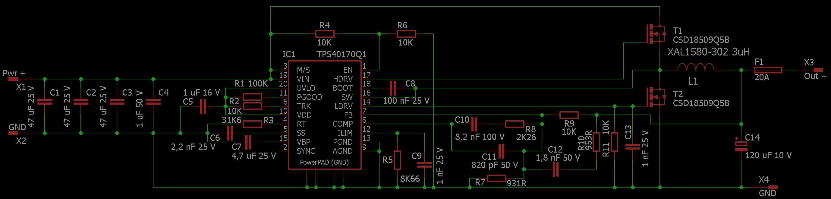
Well, it did not explode - a good start. For my it seems 1:1 as in Webench, but maybe you can find a difference, causing it to malfunction. With Vin applied (14.8V) the Vout stays at about 2V for unlimited time. As I power it up from laboratory power supply I can easy change the Vin, so when I change it, lets say go from 14.8V to 12V, suddenly the output becomes about 5V. If I put the Vin back to 14.8V - Vout changes to about 6V. Though it never reaches the needed 7V. Voltage on FB pin is about 0.5V, which I suppose means, that FB divider is OK, at 7V output it should be targeted 0.6V. But the TPS40170 is not increasing the Vout. Strange thing - HDRV has a very strange pattern, LDRV is just a straight line at 0V. Naturally, SW is also abnormal...

HDRV (Vin 15V, Vout about 2V):

Closeup of one pulse:

LDRV, same conditions:

LDRV zoomed out, to show spikes:

SW signal. At this point I lowered Vin from 15V to 11V, somewhere at approximately 12V it began increasing output voltage. SW already at increased voltage:

Lots of spikes, a little zoomed view, for more precise period/frequency calculation:

And one spike zoomed:

PCB should be exactly as in Eagle schematics, so I exclude the mistake here. Parts are also checked and seems to be OK. What else ? I would try to desolder the transistors (to measure clean signal controlling the transistors), but I think this way TPS wouldn't be working at all, right ? Anyway, I would be grateful for all ideas, it cant be that Webench made a faulty schematics second time...

Best regards

Dainius

  • Hello,

    First, please power everything off, I would first check with a DVM on Diode setting and make sure the MOSFETs are good.  Should read a Diode Drop from Source (Red) to Drain (Black). Also Check both ways on DVM from Gate to Source (Red and black and Visa versa) on the lower MOSFET.

    Also check continuity from LDRV to Gate of MOSFET in particular, but can check the resistances

    If all check out OK,  power on, and then check the inductor current to ensure you are not in an over current condition?  Can you also check the the VDD and the SS voltages please?  

    If all of the above seems OK, we may need to check your layout?  did you follow the guidelines in the datasheet for layout?

    Thanks.

  • Hello David,

    Thanks for your support and ideas. Checked the voltage drops first thing, so MOSFETS should be good. Rechecked now: high side 0,453V, low side 0,424V, reversed - high side 1,924V, low side 1,241V.

    Continuity from HDRV and LDRV to gates is OK.

    Without any load on the end there should be almost no inductor current, right ? The only thing on the end is Cout and feedback circuit. How can I check the current ? Cut the PCB trace between MOSFETs and inductor and connect ammeter there ?

    VDD:

    Some spikes can be seen on plot, though average is about 3V. Closeup of the spike:

    The SS:

    Seems to be charging up to about 1V. Zoomed view:

    Layout should be OK, I tried to follow the guidelines. Though if nothing helps - we can look. Maybe there will be something I missed.

    Best regards

    Dainius

  • Hi Dainius,

    Looking at your SS, it looks like its being reset, which suggests it is likley a current limit event.  Check your Rlim value and also your Resistor from Gate to Source on the Low side MOSFET.  Also check VBP voltage and also check that the UVLO threshold is being exceeded?

    Assuming it is an over current event, measure the current by lifting one side of the inductor and placing a wire loop and current probe, if you dont have a current probe, the you can place a current sense resistor in series with the inductor and measure the voltage, knowing the current in VRsense/Rsense.

    Hope this helps?

  • Wow, I am completely lost... Or Webench calculates cosmic formulas... I dont get it. The formula from TPS40170 datasheet:

    Rlim = (Ioc*RdsON)/9uA

    Lets make a calculation for 20A, with 2 mOhm RdsON (from transistor datasheet):

    Rlim = (20 * 0.002) / 0.000009 = 4444.44 Ohm = 4.4 kOhm

    Why did Webench calculated 8.66 k ?

    Ok, lets read the TPS4017 datasheet a bit further. On the page 30 there is schematics of 5V @ 6A. Same formula:

    Rlim = (6 * 0.011) / 0.000009 = 7333.33 Ohm = 7.33 kOhm

    Not even near to 12.1 kOhm, given in schematics.Its not the nearest standard value... So, how is Rlim calculated ? All I can find is incorrect.

    From the formula, ir seems, that with increasing Rlim resistance the limited current is also increased. With Webench recommended value and formula from datasheet current limit is 39A.

    The resistor on LDRV, the one which sets the SCP multipier value is 10k, so the SCP multiplier should be ~3, and SCP current 39*3 = 117A. Nonsense...

    UVLO - Webench just connected it to VDD, as I do not need this function.

    VBP seems to be correct, about 8V (with some fluctuation):

    Best regards

    Dainius

  • Hello Danius,

    In short, you have to take the peak current in the inductor. IOC in the Datasheet does not equal output current. It equals the output over current level, this is the peak inductor current multiplied by some factor (1.3) to give you some headroom, so as to avoid false tripping. Please follow Equation 39 and 40 in the datasheet for the correct value of RLIM.

    Hope this helps?