This thread has been locked.

If you have a related question, please click the "Ask a related question" button in the top right corner. The newly created question will be automatically linked to this question.

TPS55330: SEPIC Configuration

Part Number: TPS55330
Other Parts Discussed in Thread: TPS55340, LM5175, LM5118, CSD88539ND, LM25118

Hi There, I'm wondering if you have an example of the TPS55330 regulator in SEPIC configuration. 

I'm looking to use run device as a 3.6V, 5A Buck-Boost converter (with input 2.9 - 4.5V), and SEPIC would seem like a good choice, but the datasheet has no info regarding designing in this config. Any help would be appreciated!

Many Thanks,

Dave

  • Hi, I found some help here:

    www.ti.com/.../slva516a.pdf

    There's also an Excel spreadsheet for the TPS55340 here:

    www.ti.com/.../slvc433

    Based on the calcs in the spreadsheet, I'm wondering is it possible to build a 5A supply with this converter in SEPIC config and these specs:

    Vin = 2.9 - 5V, Vout = 3.6V, Imax = 5A

    The switch can handle 5A, but I'm struggling to choose components to realise a 5A solution.

    Any ideas?

    Thanks,
    Dave
  • Hi Dave,

    In a SEPIC, the switch must conduct the input current + the output current. So at the minimum input voltage (assuming 100% efficiency and ignoring ripple current) the switch needs to conduct (3.6 V/2.9 V * 5 A) + 5 A = 11.2 A. Once you include the losses and ripple this required peak current goes up to maybe >15 A.

    For this much current, you may be better off looking at a 4 switch buck boost solution instead of a SEPIC. I believe the closest we have to get this much current from a buck boost would be the LM5175. However I must admit I do not regularly look in this area so I'm not aware of all of the possible solutions. You may want to try making a new post putting your input voltage and output voltage/current requirements in the title.

    Best Regards,
    Anthony

  • Many Thanks Anthony, the switch current explains a lot.

    Many thanks for the advice regarding the LM5175. One thing that I'm still a bit confused about is why there is an output current limit on the non-integrated controllers like the LM5175. As long as the external FETs and Inductor are chosen to withstand the correct current, is it not these external components that determine that max possible output current? Or is the drive strength of the FET gates a factor?

    Which leads me to my second question - the 2A gate drive spec on the LM5175. I would have assumed the gates would be high impedance and require very little current for switching. Am I mistaken here?

    Many thanks for your support :)

    Cheers,

    Dave

  • You may still want to set a current limit for fault protection.
    When the gate is driven from low to high, you will still have significant current during the turn on time as the total gate capacitance is charged.
  • You're right in that it depends mainly on the external component selection. You could say these limits are more of recommended limits but in reality the limit will vary from application to application. The drive strength is usually the main factor leading to the recommended limits.

    The current for the gate driver is usually a peak current occurring when turning on/off the MOSFET. The gate drivers need to be capable of driving very high peak currents to turn the MOSFETs on/off more quickly to reduce switching loss. The high peak current is needed because the driver needs to charge/discharge the gate capacitance of the MOSFETs. As a simplified example, if the driver had to charge up 1 nF of capacitance to 5 V in 10 ns it would take 0.5 A of average current. In reality the gate driver is not outputting a fixed DC current the entire time it is charging/discharging the gate of the MOSFET.

    The gate driver current spec is something that can be used to compare how quickly a driver can turn on/off the MOSFETs. Sometimes this spec is based solely on the resistance of the pull up and pull down switches use in the gate driver. On some other parts you may actually see the gate drive strength specified as gate drive pull up/pull down resistance instead.

  • Thanks Anthony, thanks John.

    So based on the gate driver being the limiting factor from an output current point of view, is there a way to convert this gate driver spec into a 'recommended max output current' spec? Also, based on my design requirements of 2.8 - 5V Input, 3.6V Output, 5A Max load, do you guys have any suggestions for non-inverting buck-boost controllers? Even 3 - 5V input might be OK. Am guessing something with gate drive of ~2A would be adequate?

    Many thanks,

    Dave
  • Hi Guys,

    Following on from the discussion above;

    The LM5118 looks good to me for my 3.6Vout, 5A reg. 3 - 42V input voltage asynchronous buck-boost. Gate Drive = ~2A. If I chose something like CSD88539ND for the FET switches (Gate Charge = 9.4nC, Drain Current = 15A) and switched at 500kHz, is it correct to say that the Gate Drive Current would need to be I = Qf = 10nC x 500kHz = 5mA to switch correctly and efficiently? And how does this figure vary with load current?

    Many Thanks,
    Dave
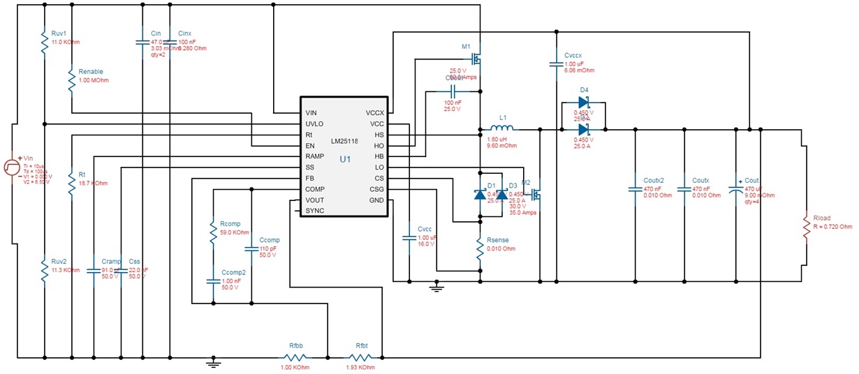
  • Webench has allowed me to generate a design, which I'm taking as a positive sign! What do you think? (3 - 5V Input, 3.6V Output, 5A Load)

  • Hi Dave,

    Something to keep in mind with the gate drive current you calculated is this is the average current. There are still spikes in the current when the MOSFETs turn on and off.

    It is a good sign that WEBENCH gave a design for this. However I tried to get WEBENCH to generate a design to take a quick look myself and it wouldn't let me. Are you sure you had put in the right input voltage for your design? You may want to make a new post with the LM25118 part number in the title. This should get the attention of someone who is more familiar with it.

    Best Regards,
    Anthony
  • Thanks Anthony. One final question regarding the LM25118. I've just noticed the VCC UVLO specs in the datasheet - it states lock out will occur at 3.7V. Am I correct in assuming that this means that if my Input voltage is say 3V, output is 3.6V, that the Vcc and thus the gate drivers will not work correctly? Do I need an extra 4.5V supply? 

    Many Thanks for your help,

    Cheers,

    Dave

  • Hi David,

    If the VCC voltage is below 3.7V the gate drivers will not operate and switching will stop. So in the condition described above the there will need to be an external supply for the VCC pin. An external supply for VCC is also recommended to ensure start-up when the input voltage is below 5V.

    -Garrett