This thread has been locked.

If you have a related question, please click the "Ask a related question" button in the top right corner. The newly created question will be automatically linked to this question.

Implementation of -5V turn-off of Highside SiC MOSFET in a Halfbridge topology using 25V Bootstrap power supply

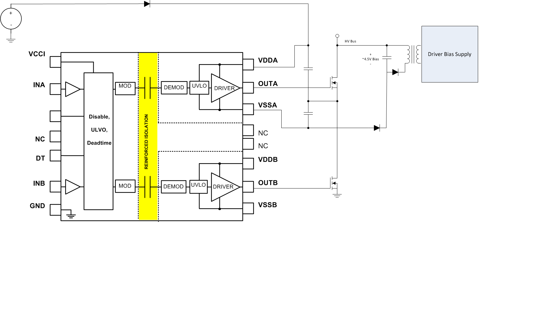
Currently, I am working on a SiC half bridge circuits, and trying to use bootstrap power supply instead of isolated supply for highside and lowside switches. But it seems that the implementation of the -5V turn-off for highside switch is an issue. 

Can someone give me some hints to solve this problem?

  • X.V.,

    I have asked an AE to give some comments on this request, look for a response forthcoming.
  • X.V.,

    You are correct -- generating positive and negative drive using a bootstrap technique is not straightforward. I actually will need to think about this one for a day or two and consult with my colleagues to give you a suggestion. As you know, you should be able to turn the SiC device off without the negative drive voltage. There is a performance trade-off, but it will simplify your design.

    In general, every time I have used negative drive on the high-side power switch in a half-bridge, I have used an isolated supply. 

    While I work on this, please let me know if there is a specific TI driver that you are targeting for your design or any other design details that may be revelant.

    Your patience is appreciated,

    - Daniel

  • Hello XV,

    There are a couple of ways to generate a positive and negative drive voltage for the SiC MOSFET without having both bias supplies isolated and floating with respect to the switch node.

    The easiest to implement is to have a zener and parallel capacitor between the driver and the gate, this diagram can be seen on page 33 of the UCC21250 datasheet.

    This circuit does have limitations regarding duty cycle range (low duty cycle may not full charge capacitor), initial cycles do not have negative drive until capacitor charges, and negative drive cannot be maintained for long off times.

    Another idea using the bootstrap concept is to have a normal bootstrap supply for the positive voltage, and a bias supply referenced to the high voltage rail to source a negative bias bootstrap. See diagram below. The positive supply is charged when the low side switch is on, and the negative supply when the high side switch is on. This does require a single isolated bias, but the supply output is not exposed to high dV/dt as with the bias supplies referenced to the switch node. Care needs to be taken to prevent overcharging of the high side floating capacitors, it is advised to have limiting resistance in series with the diodes, and limiting zener diodes may be required.

  • X.V.

    I am reposting since the illustrations did not show on the web. See below.

    • Hello XV,

    There are a couple of ways to generate a positive and negative drive voltage for the SiC MOSFET without having both bias supplies isolated and floating with respect to the switch node.

    The easiest to implement is to have a zener and parallel capacitor between the driver and the gate, this diagram can be seen on page 33 of the UCC21250 datasheet.

    This circuit does have limitations regarding duty cycle range (low duty cycle may not full charge capacitor), initial cycles do not have negative drive until capacitor charges, and negative drive cannot be maintained for long off times.

    Another idea using the bootstrap concept is to have a normal bootstrap supply for the positive voltage, and a bias supply referenced to the high voltage rail to source a negative bias bootstrap. See diagram below. The positive supply is charged when the low side switch is on, and the negative supply when the high side switch is on. This does require a single isolated bias, but the supply output is not exposed to high dV/dt as with the bias supplies referenced to the switch node. Care needs to be taken to prevent overcharging of the high side floating capacitors, it is advised to have limiting resistance in series with the diodes, and limiting zener diodes may be required.