This thread has been locked.

If you have a related question, please click the "Ask a related question" button in the top right corner. The newly created question will be automatically linked to this question.

UCC28180: Power-on switching delay

Part Number: UCC28180

The evaluation board for this part has a diode across "inductor + PFC diode".  My circuit below does not have this inrush current steering diode and it has been working fine.

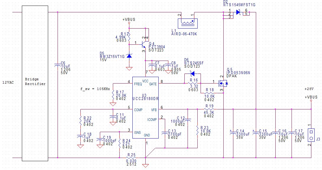
When power is turned on, in-rush current goes to about 25A.  Since my inductor's I_sat is 15A, if switching started during inductor saturation, FET current will be high and I was expecting to see Peak Current Limiting kick in.  But what happens is Gate switching does not start until the initial inrush current has gone down.  (VCC goes above V_UVLO long before this BTW.)  This is a good thing but I didn't know why this delay existed.  Then when I looked at the ICOMP pin, that gave me a clue.

In the scope capture shown below, top trace is GATE, middle trace is ICOMP, and the bottom trace is inductor current.  It appears that inrush current causes ICOMP to saturate and prevents Gate switching.  When ICOMP comes out of saturation, switching starts.  This is perfect if this behavior is what the chip is designed to do.  If so, then why the diode across "inductor + PFC diode" ever needed?

Thanks,

  • Hi JC88

    The bypass diode is used so that the inrush current does not flow through the PFC diode (D2 in your schematic). The PFC diode in the CCM boost topology must be an ultra fast (or, in off line applications sometimes a SiC type is used) and these parts may or may not be rated to carry the inrush current. I'd suggest that you look at the 210A non-repetitive peak surge current rating (IFSM) of your diode and compare it to your inrush surge. It looks like your diode is ok in this regard and you won't need the bypass part but it isn't always the case - it just depends on the part being used - .

    You should also look at the peak negative going voltage at the ISENS pin - you may need to add a clamp to keep it more positive than -1.1V - see section 8.3.14 in the UCC28180 datasheet for more details www.ti.com/.../ucc28180.pdf

    Regards
    Colin
  • Hi

    Thanks for your enquiry on the UCC28180. I have asked one of our application engineers to respond to your question. You should see a reply later today.

    On the UCC28180 a diode must be fitted between the CS pin and GND to limit the negative voltage to less than a diode drop during the inrush event.

    Regards

    Peter